Inspired by all the cool high-speed shots on Mythbusters, I just had to have a high-speed camera. However, base models start at about $12,000 (at the time), obviously way too expensive. So, I decided to make my own. Mike’s high-speed camera controller gave me a lot of inspiration to try this. This was my first significant project in programmable logic devices, I did a little bit of work with PAL chips when I was at BCIT. This project was done mainly in 2007-2008 while I was finishing/just finished BCIT, and I would say I learned more doing this project than during my entire time at BCIT.
The camera is based on the LUPA300 high-speed image sensor from ON Semiconductor (formerly produced by Cypress). It’s capable of 640×480 @ 250fps, and increased speed at lower resolution, eg. 320×240 @ 940fps. The four internal ADCs operate at 20MSa/s, muxed to a 10-bit output bus clocked at 80MHz.
The camera is basically a small daughterboard containing the image sensor and power supplies, connected to a Spartan 3A FPGA dev board. Video is stored uncompressed in the 64MB DDR2 RAM, allowing a paltry 1s of record time, but sufficient for most high-speed video work. The board has various interfaces such as 10/100 ethernet, VGA, an RS232.
The camera can operate standalone with a monitor, via an onboard ASCII UI running on a Microblaze CPU. Alternatively (most often actually), the camera is operated and video downloaded remotely over Ethernet, controlled by a PC application written in C#.
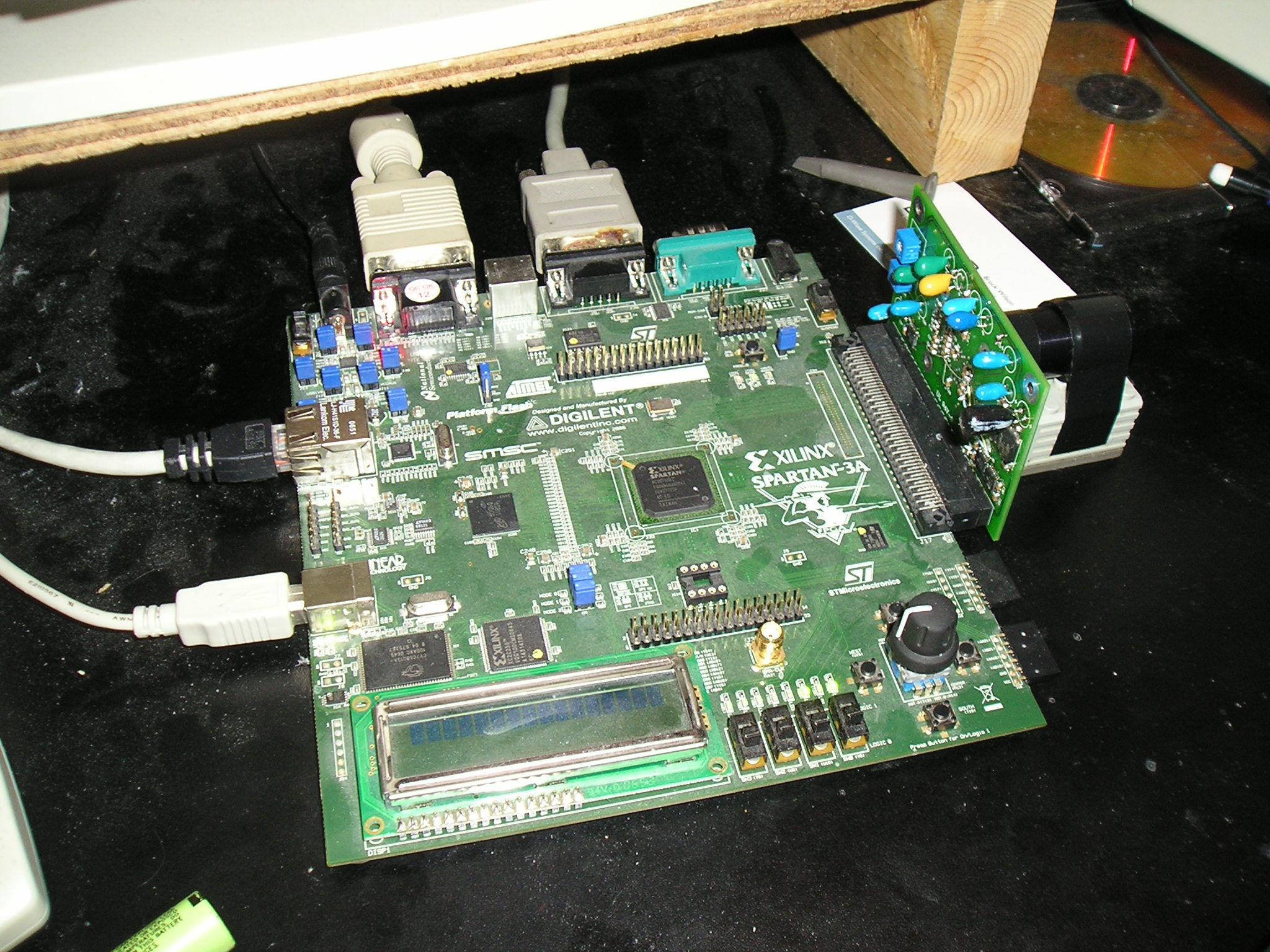
Figure 1 – Prototype during development. Note the lego motor holding the lens
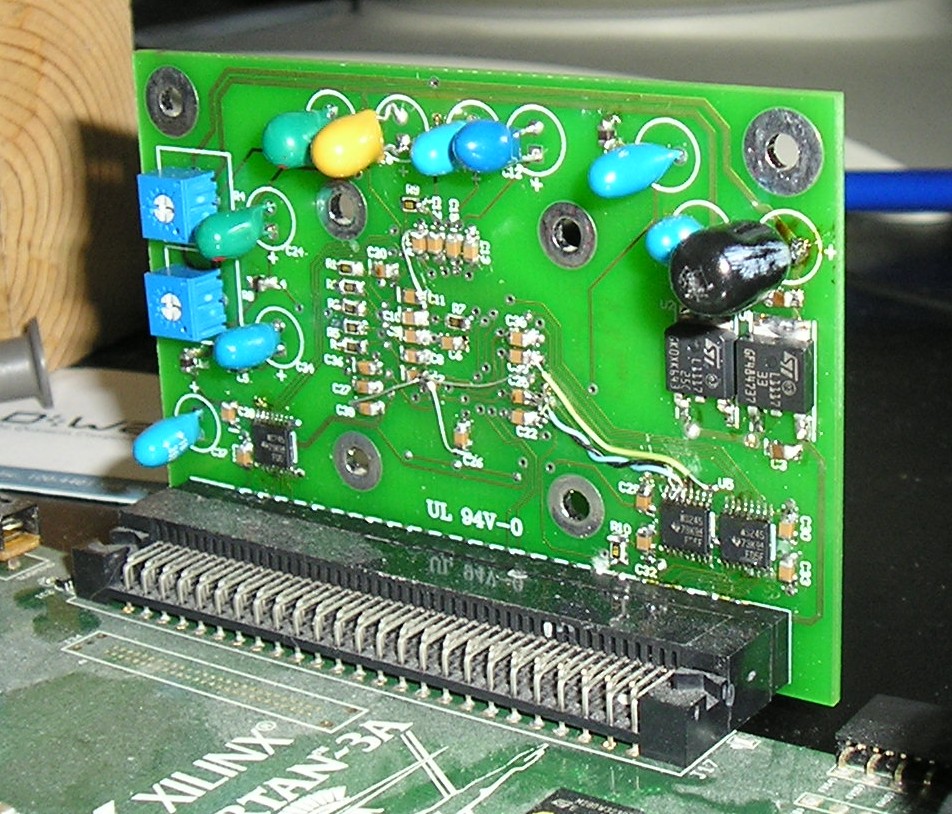
Figure 2 – Back of image sensor daughterboard. Mods are to correct for signal integrity issues.
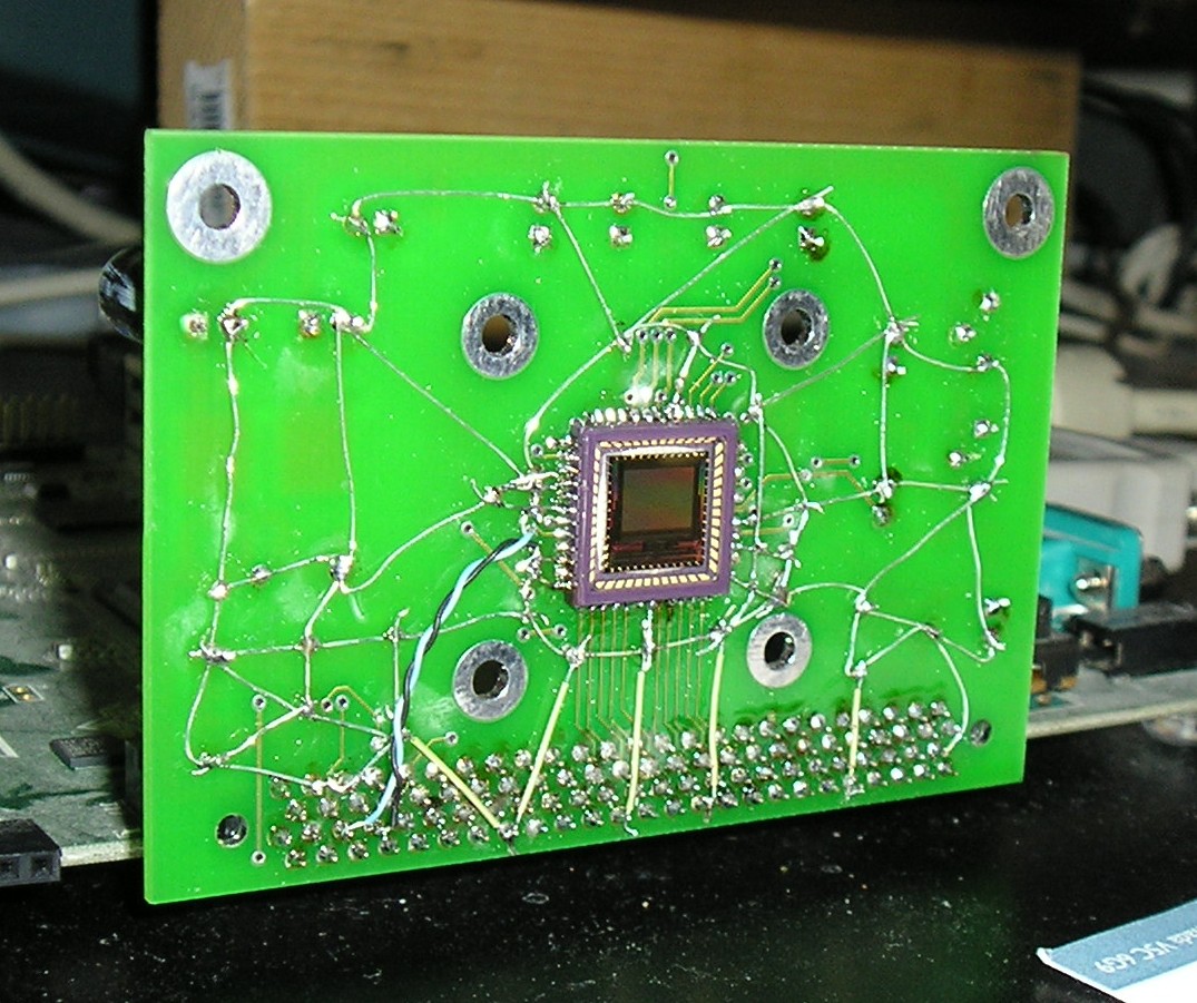
Figure 3 – Daughterboard front showing image sensor and ground “grid” to compensate for missing ground plane on PCB. Never submit anything but Gerbers to PCB manufacturers!
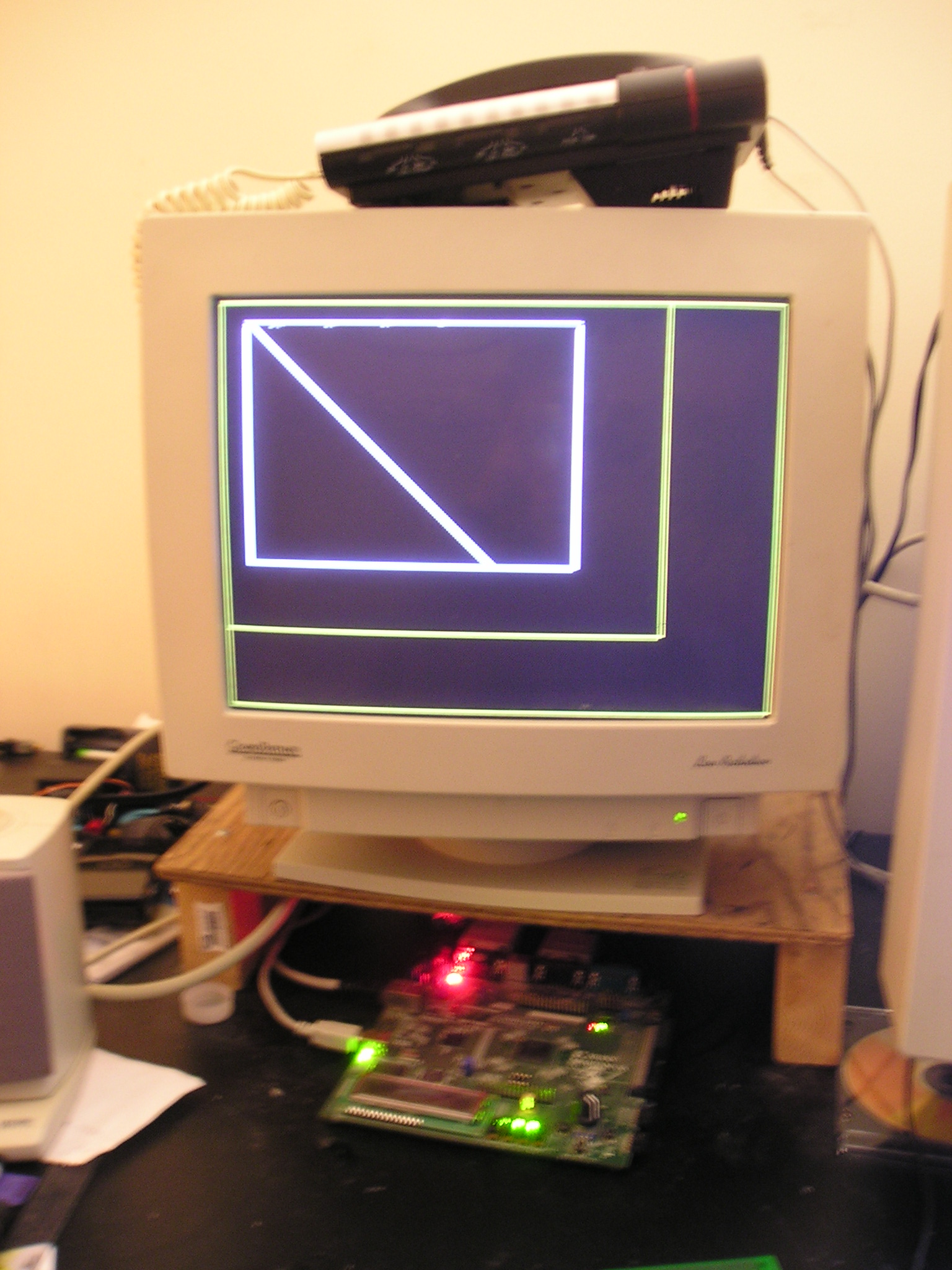
Figure 4 – Testing the video display verilog code with the famous “box and diagonal line” test pattern. Some bugs visible near the top.
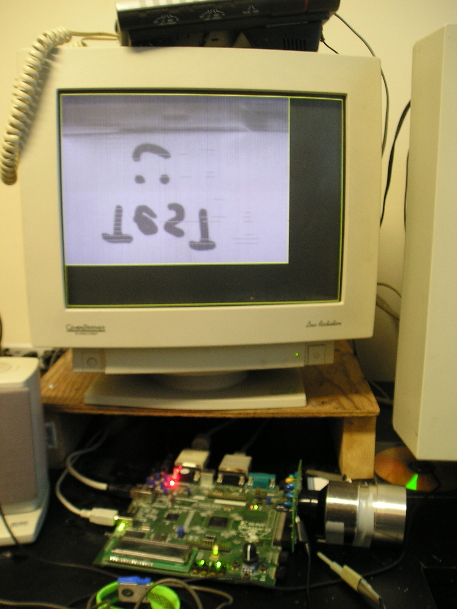
Figure 5 – Testing the image sensor data write hardware
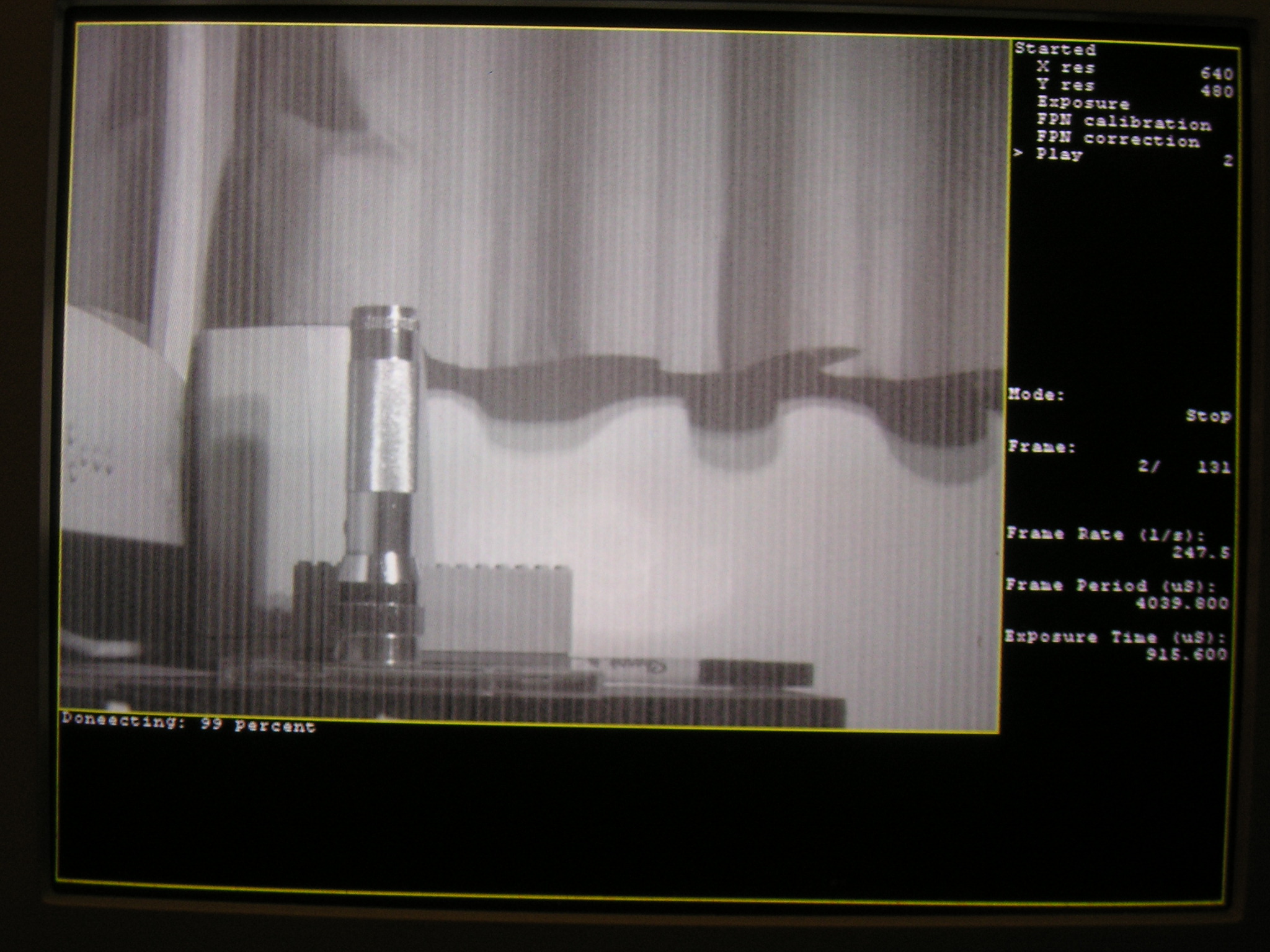
The data coming off the image sensor is 10-bit and needs some processing to be usable. Per pixel offests need to be subtracted to compensate for fixed-pattern noise (FPN) which plagues CMOS image sensors. After FPN correction, the data needs to be gamma corrected to match the display gamma. The values coming off the ADC are linear, ie. they are proportional to the amount of light hitting the pixel. The typical 0-255 RGB values used on computers are nonlinear sRGB values, so a blockram based lookup table converts the 10-bit ADC values to 8-bit output values ready to display. Unlike most high-speed cameras, this image processing is done live as the data is read off the sensor. Offsets are read out of DRAM, subtracted from the ADC output data, gamma correction is applied, and the data is written back to DRAM fully processed and ready to display.
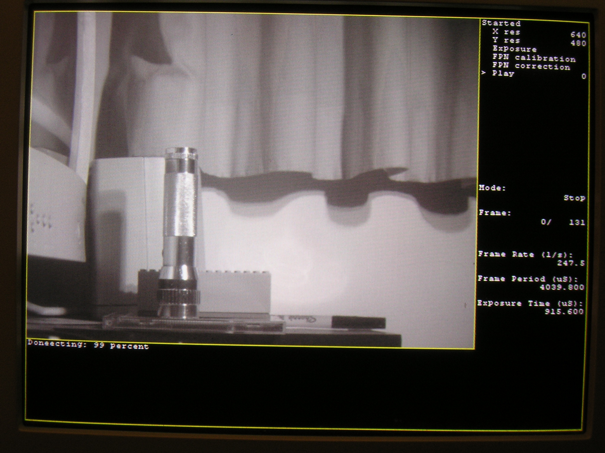
Figure 6 – Imaging data path working properly, and an example of an (older) menu. Note the improper clearing of the terminal on the bottom. This is an example of the same image with FPN correction disabled.
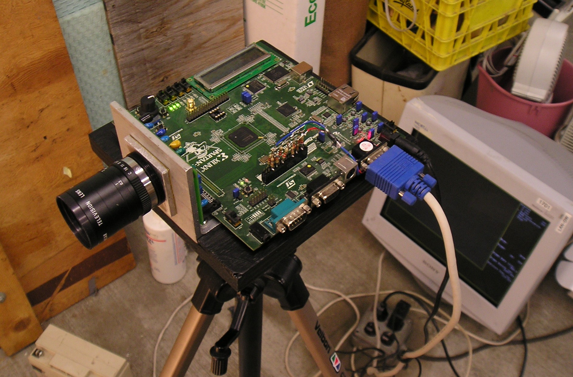
Figure 7 – Completed camera
Video 1 – Very first video downloaded off the camera. Record mode: 320×240 940fps, 457uS exposure time, playback rate 30fps
Lighting: 2 * 100W Halogen ~40cm away
Video 2 – Compilation of videos, all taken on this camera
Source files coming soon!