Sevcon Gen4 AC motor controller teardown

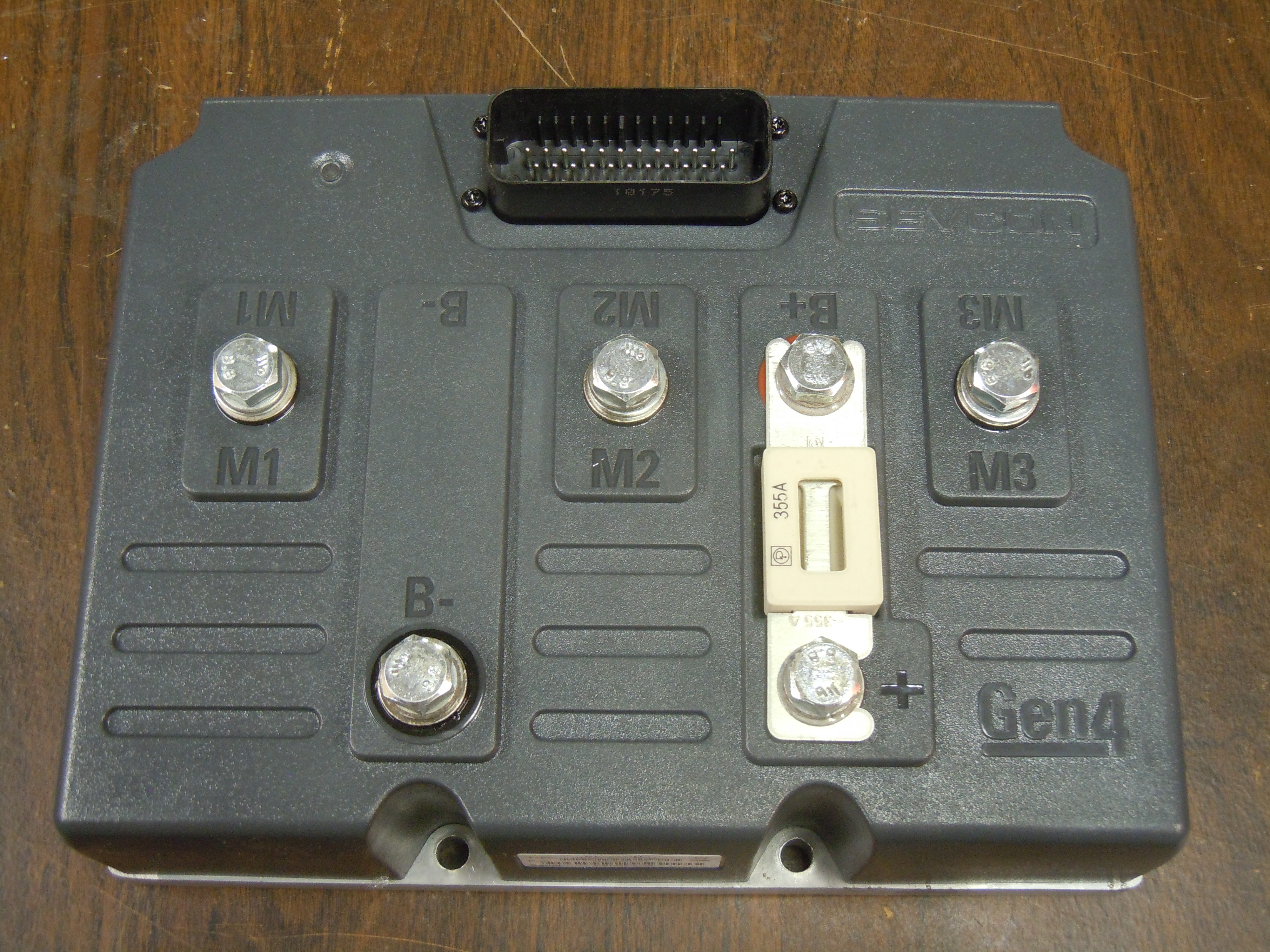
Here’s a look inside a Sevcon Generation 4 AC motor controller. This particular one is the 80V 350A model, sourced for the ArcWolf racing go-kart. Two were purchased from an eBay seller in located in Korea for US$720 total including shipping.

Imgur album of all teardown photos

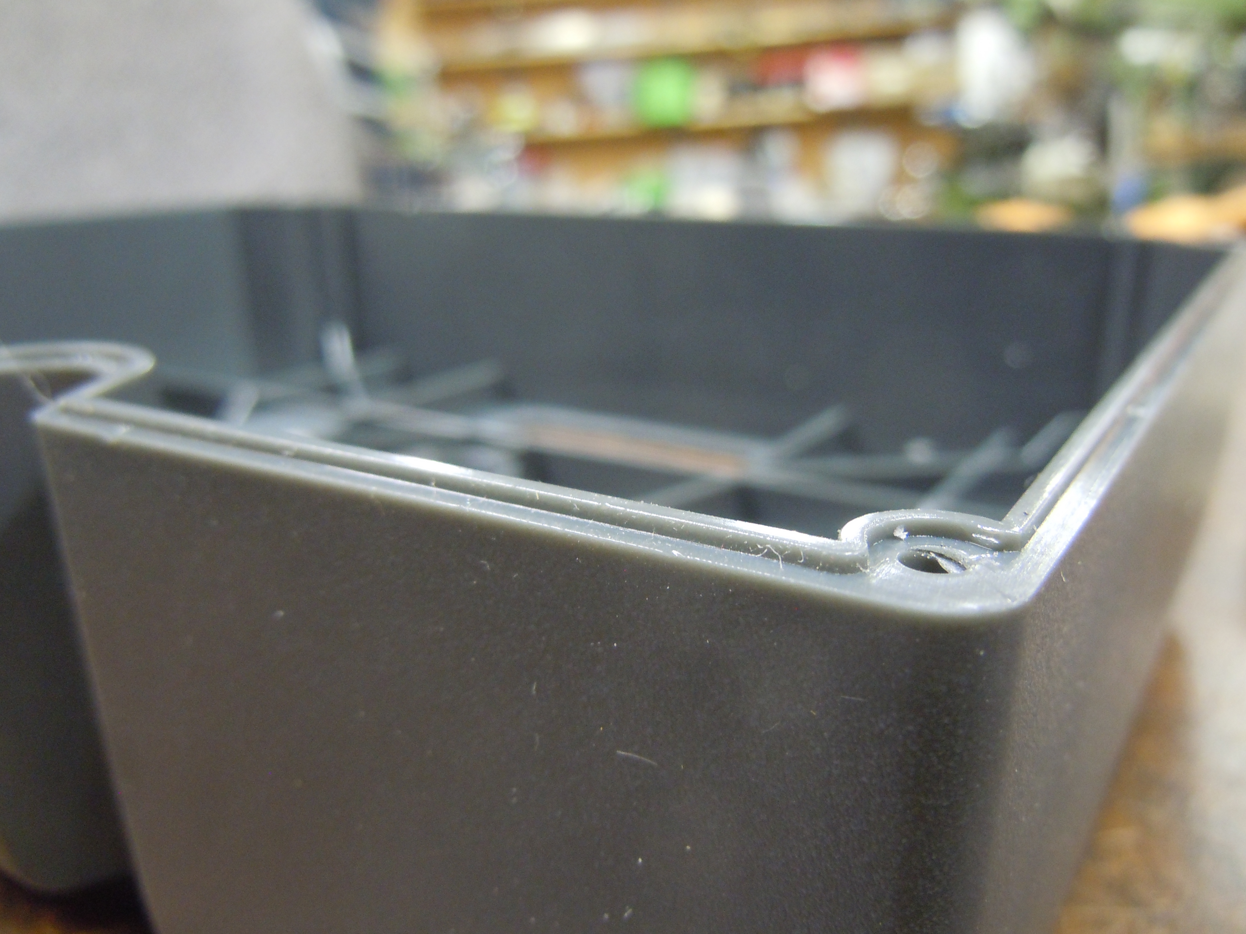
The controller is waterproof with a plastic shell over an aluminum base plate. Terminals protrude through the top.
DSCN4758

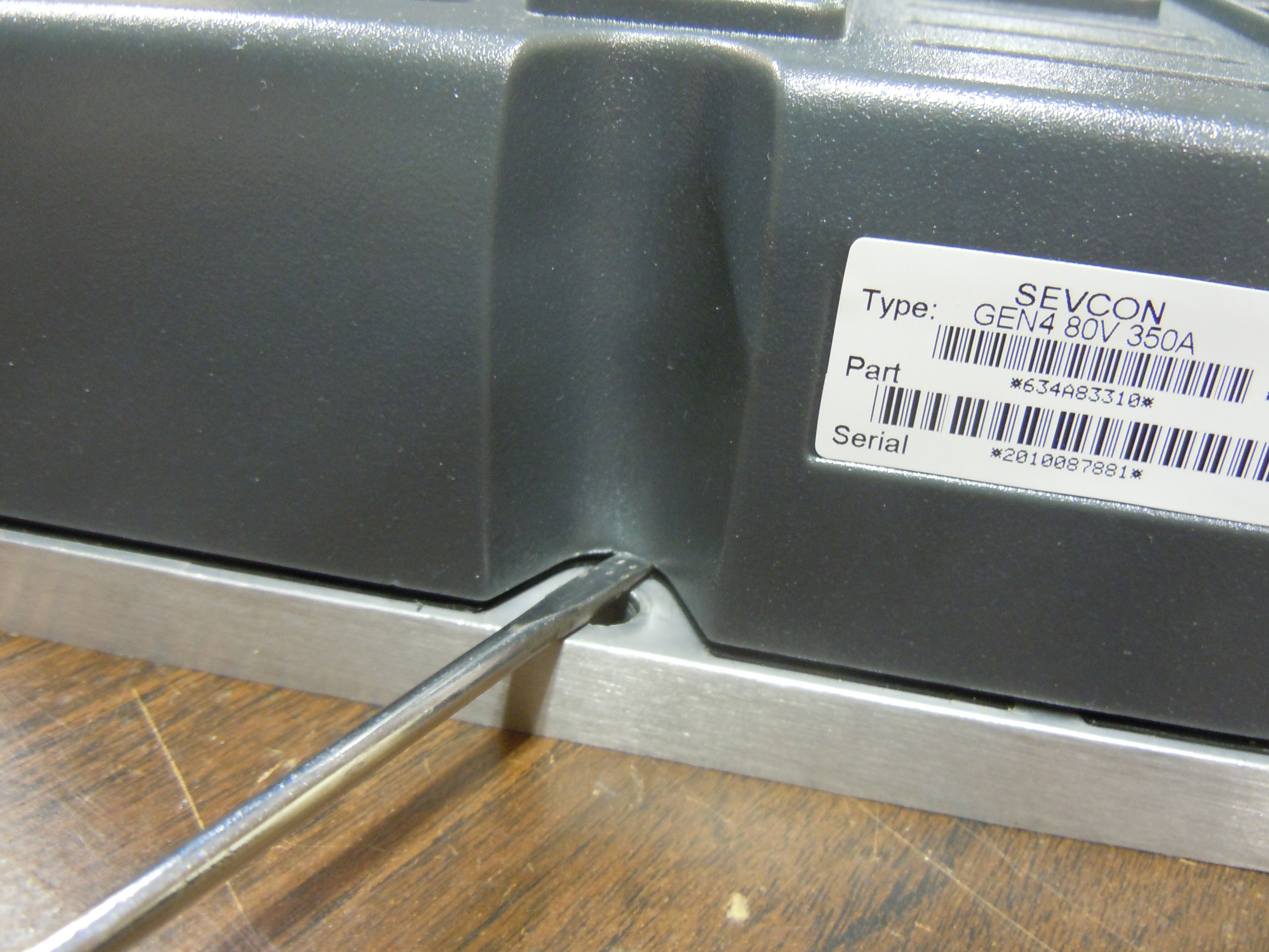
With the screws removed, the top comes off with prying.
DSCN4759

DSCN4763

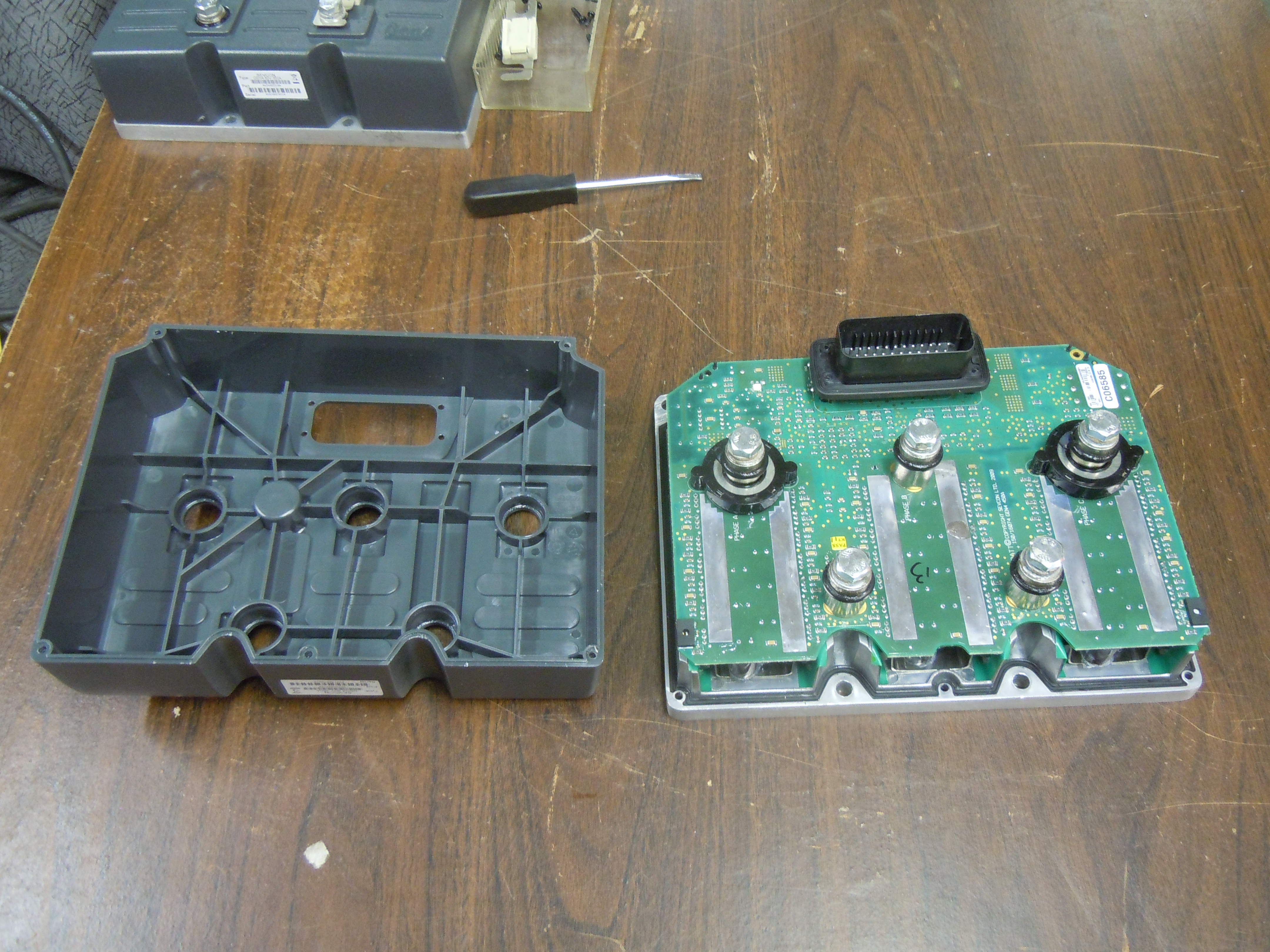
Just one big board. Surprisingly there are no bus bars, the 350A connections go directly to the PCB! The three half bridges are clearly visible. Each leg uses seven IPP075N15N3 G 150V 7.5mOhm FETs.

The PCB is at least four layer. The top and bottom layers both carry the current from the FETs to the 3 phase outputs, with the DC bus running on inner layers. The number of inner layers is not known.
DSCN4765

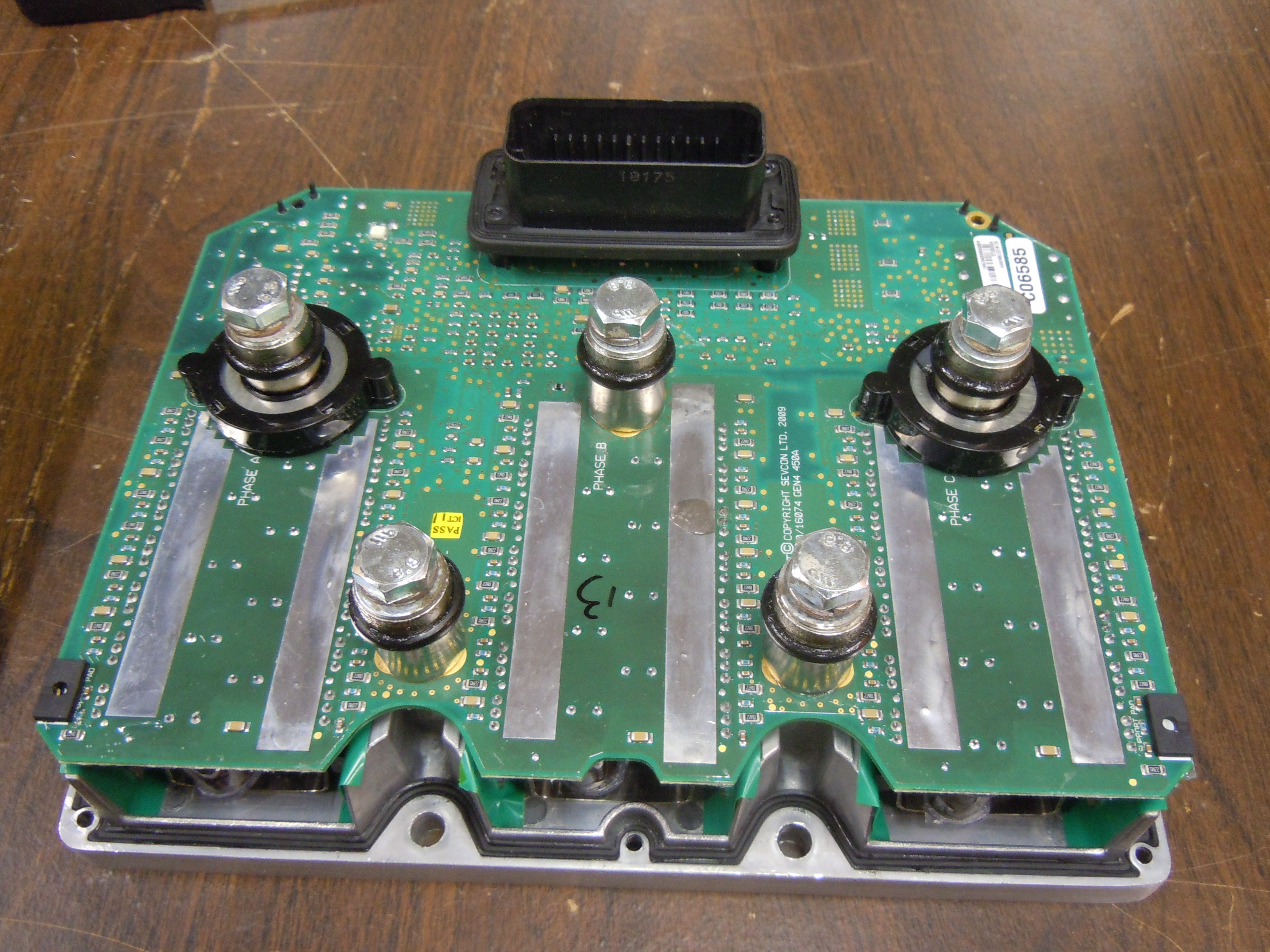
The FETs are clamped to the heatsink by spring clamps. These must be held open with a special jig during assembly while the top board is inserted.
DSCN4778

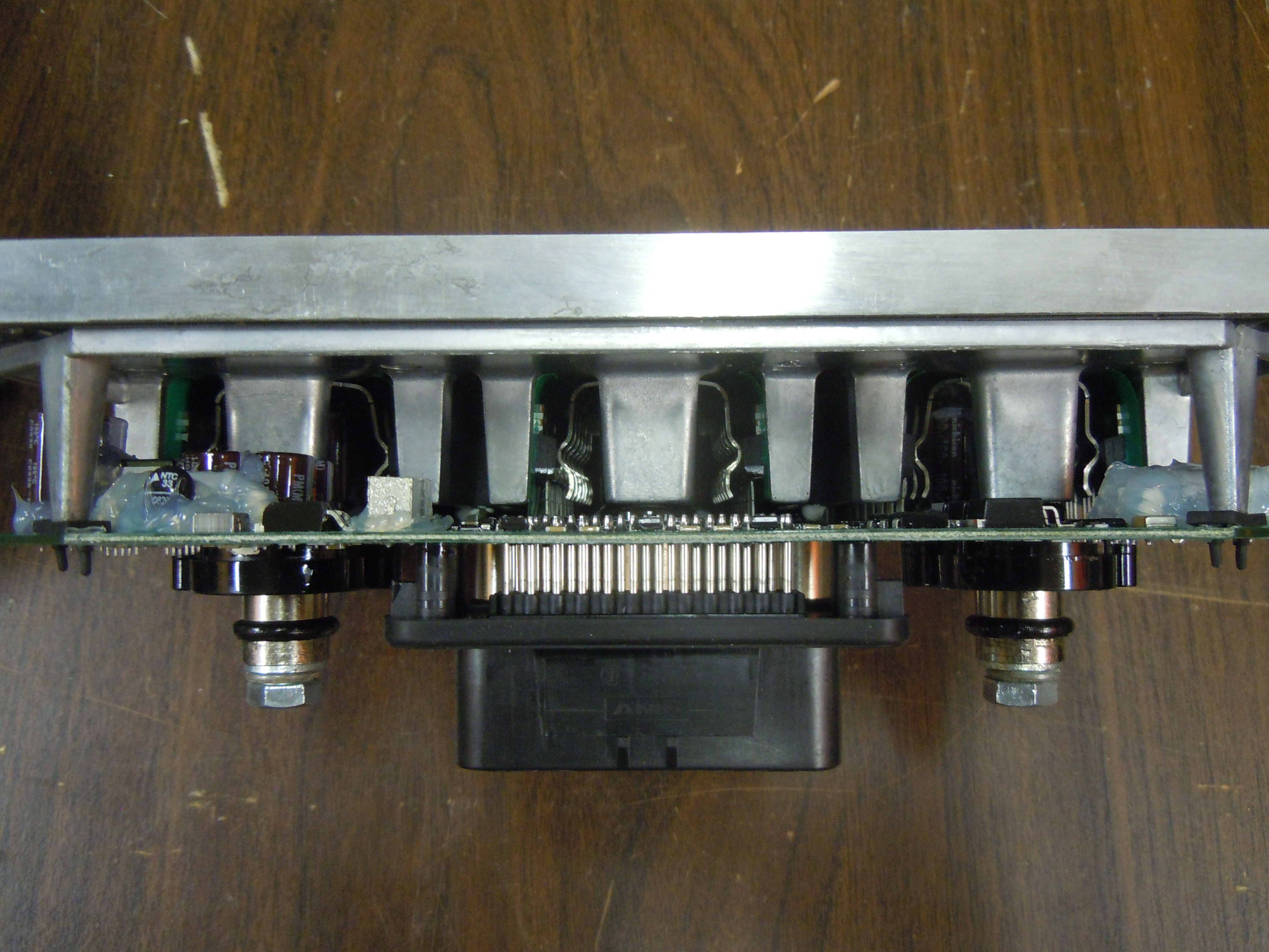
A green thermal interface material couples heat to the heatsink. The material is basically a think Kapton sheet with a phase change material that melts at high temperature. I recall using this material in an AC inverter I built years ago because it was the highest performance economical material available. It likely still is to this day.

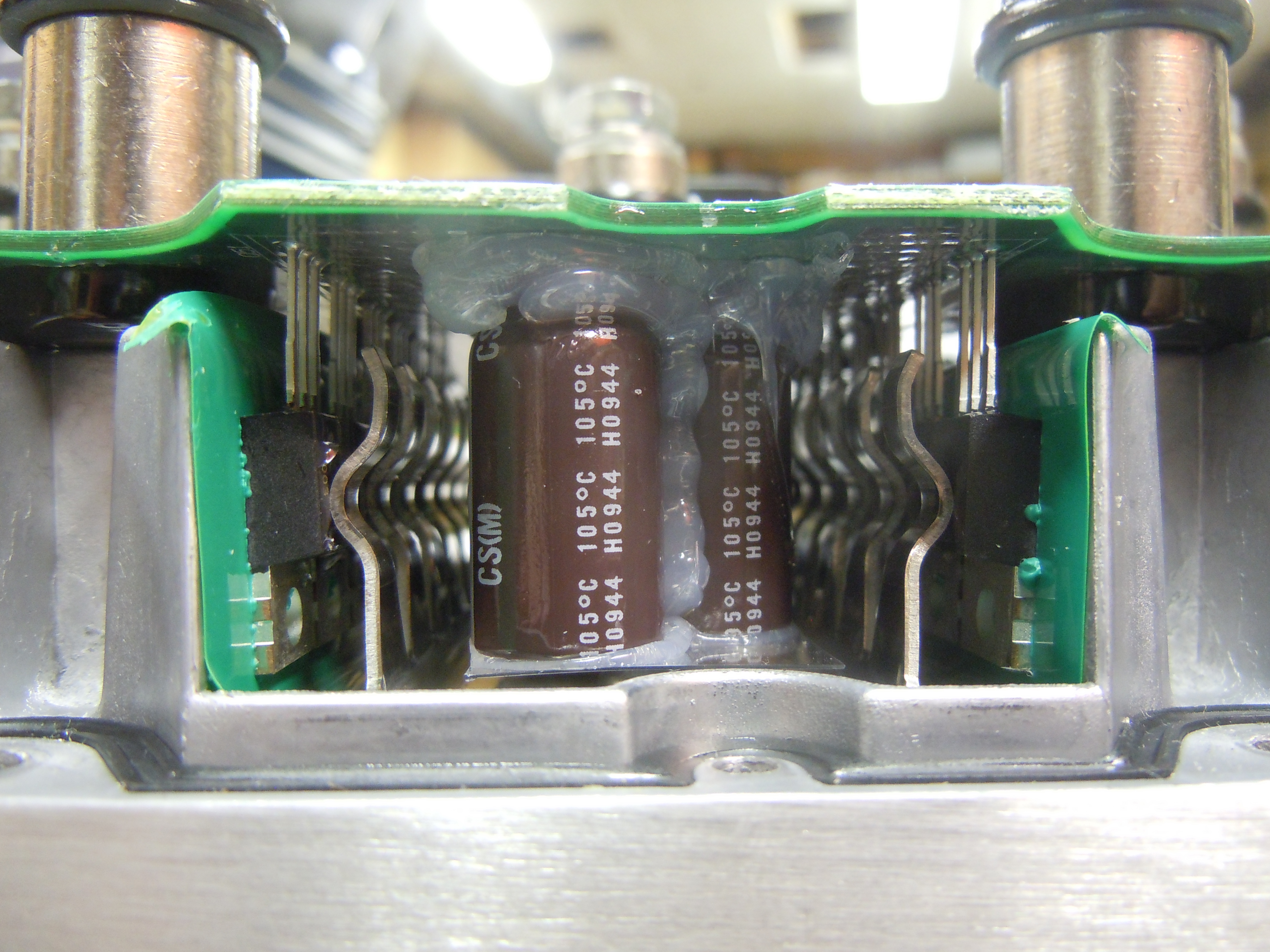
The bus capacitors are Nichicon 160V 100uF with 8 per leg (2400uF total). The capacitors and other weak components are secured with silicone to stop them from breaking off due to vibration.
DSCN4789

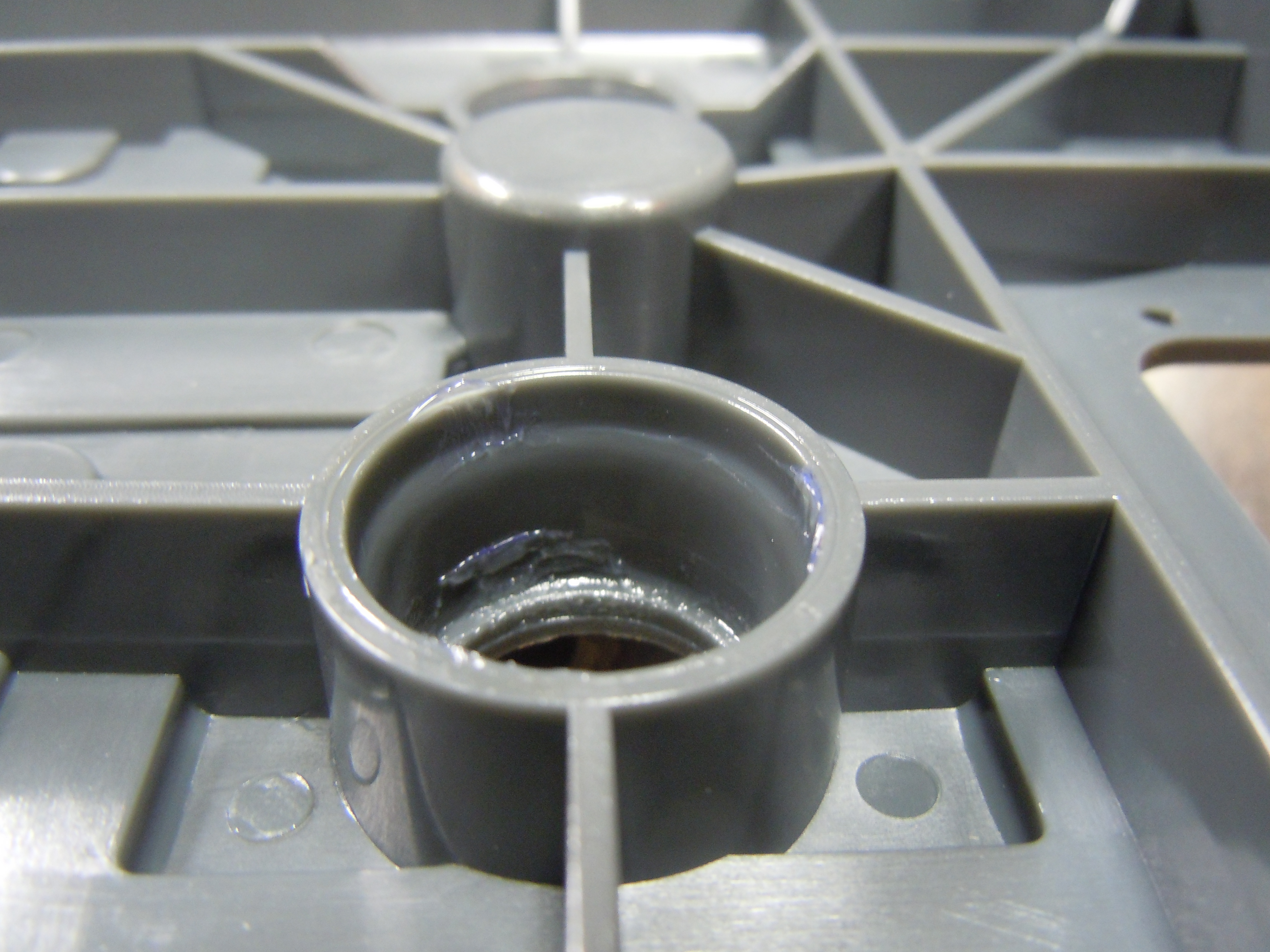
Current sensing is accomplished with hall effect current sensors. These are simply a slotted toroidal magnetic core around the power conductor.  The slot concentrates the magnetic field, allowing a hall effect sensor in the slot to sense the magnetic flux which is proportional to the current. The gap / hall sensor is under the clear silicone.
DSCN4768

The magnetic laminations are visible. For high current applications ferrite may saturate, so iron laminations are used instead.
DSCN4770

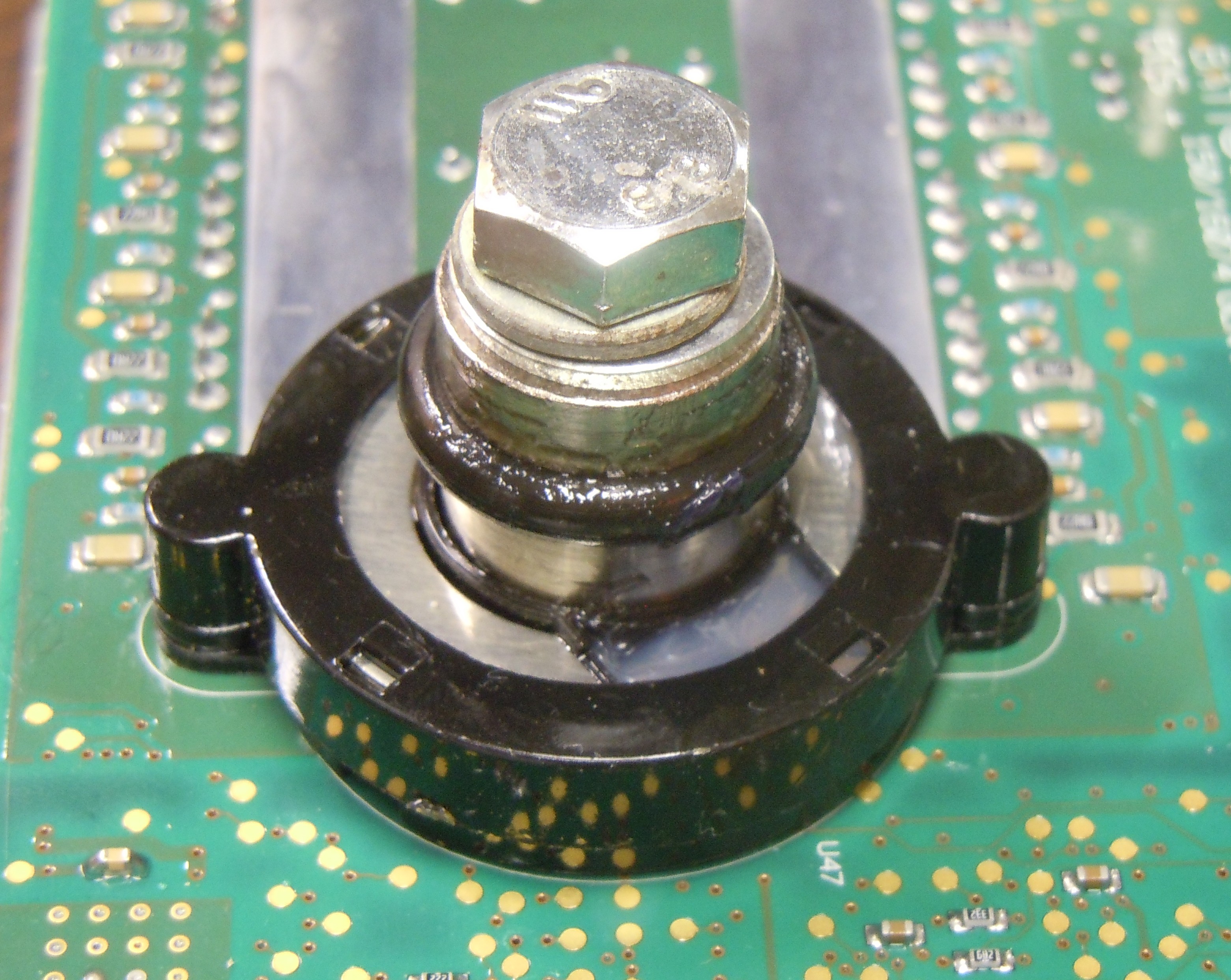
Terminals are sealed with o-rings. Grease is applied presumably to ease assembly and to improve sealing.
DSCN4772

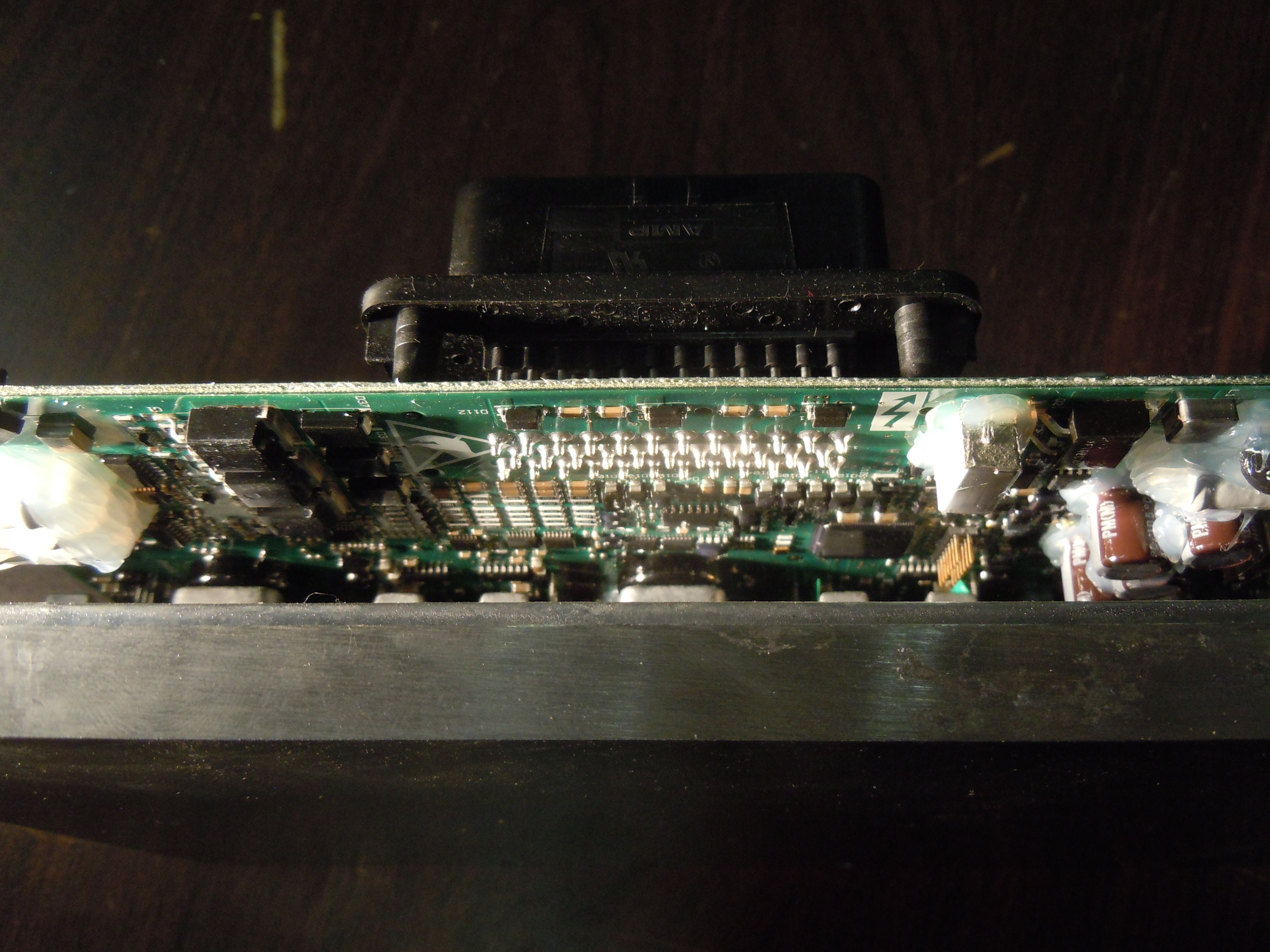
The logic section of the board is hard to see without removing the entire board. There’s not too much here, a large amount of IO protection near the connector, a switching power supply to the right, and what I believe are contactor drivers on the left.

The main micro is a TMS320F2811 32-bit 150MHz device, quite powerful!
DSCN4783

Heatsink temperature is sensed by two thermistors mounted to the main PCB and inserted into holes in the main heatsink. There are no wires in the entire design, leading to very easy and low cost assembly.
DSCN4785

The case is sealed to the base by a o-ring-like moulded rubber seal
DSCN4764 DSCN4792

Overall a very elegant and easy to assemble design.

A123 capacity and internal resistance

The 3 cells are now assembled into a pack, which will speed up testing compared to doing each individually.

6 cycles have been performed on the pack so far, and the performance has been consistently around 19Ah. On cycle 3 the pack was accidentally over discharged, causing a temporary reduction in capacity that appears to be recovering over several cycles.

Cycle  Capacity    Notes
1      19.25Ah
2      19.22Ah    
3      19.20Ah     1
4      18.28Ah
5      19.00Ah
6      19.10Ah

Notes
1. Accidentally overdischarged to <1Vpc on cell 1. Ah value includes discharge only to 2.5Vpc

The cell internal resistance averages 2.5mOhm with some spread over time and cell that’s measured. The load was varied from 20A to 36A and voltage deltas used to calculate the internal resistance. X axis on the graph below is Ah discharged from full charge.

IR test 1

Test Setup
2014-05-19_18-59-18_704

Graphs:
Pack Cycle 1

Pack Cycle 2

Pack Cycle 3

Pack Cycle 3 charge

Pack Cycle 4

Pack Cycle 5

Pack Cycle 6

Raw data: A123 Battery Data

Chinese A123 Cell testing

I’m designing a battery for our go-kart team ArcWolf Racing. Basic specs are around 88V and 30-40Ah, and one of the prime candidates are the 3.2V 20Ah A123 pouch cells, configured at 28S2P for 89.6V 40Ah.  Local sources are about $70 per cell which is very high compared to the ~$20-30 per cell available on Alibaba or AliExpress.

After looking at reviews, the seller ShenZen FHT Co. Ltd. has the best feedback, so we ordered 3 cells for testing at $30 each. They arrived within 2 weeks and were packed well (box in a box in a box!).

The test setup consists of a modified Delta-Q charger acting as a power supply, a shunt, one of my BMS prototypes as a data logger for voltage and current, and a “MacGyver” resistor consisting of bailing wire in a bucket of water.

2014-05-15_20-45-22_641

Figure 1 – Test setup

2014-05-15_21-59-51_395

Figure 2 – “MacGyver” resistor with resistance controlled by moving  green alligator clip tap

Cell 1 was charged to full capacity at 1C (20A) to 3.6V, putting 13.5Ah into the cell from its shipping state of charge. It was then discharged using the resistor down to 2.5V, resulting in 19Ah capacity.

Cell-1-Cycle-1


Figure 3 – Cycle 1 on Cell 1, starting from shipping SOC. Total discharge 19Ah. Raw data: Cell 1 cycle 1

A quick test of the internal resistance was performed, which is probably highly inaccurate. The voltage drop from rest was measured when a 25A load was connected, resulting in a 50mV drop, putting the internal resistance at about 2mOhm.

Further testing to follow with more cycles on more cells. Looking promising initially though!

HSC80 Overview

Inspired by all the cool high-speed shots on Mythbusters, I just had to have a high-speed camera. However, base models start at about $12,000 (at the time), obviously way too expensive. So, I decided to make my own. Mike’s high-speed camera controller gave me a lot of inspiration to try this. This was my first significant project in programmable logic devices, I did a little bit of work with PAL chips when I was at BCIT. This project was done mainly in 2007-2008 while I was finishing/just finished BCIT, and I would say I learned more doing this project than during my entire time at BCIT.

The camera is based on the LUPA300 high-speed image sensor from ON Semiconductor (formerly produced by Cypress). It’s capable of 640×480 @ 250fps, and increased speed at lower resolution, eg. 320×240 @ 940fps. The four internal ADCs operate at 20MSa/s, muxed to a 10-bit output bus clocked at 80MHz.

The camera is basically a small daughterboard containing the image sensor and power supplies, connected to a Spartan 3A FPGA dev board. Video is stored uncompressed in the 64MB DDR2 RAM, allowing a paltry 1s of record time, but sufficient for most high-speed video work.  The board has various interfaces such as 10/100 ethernet, VGA, an RS232.

The camera can operate standalone with a monitor, via an onboard ASCII UI running on a Microblaze CPU. Alternatively (most often actually), the camera is operated and video downloaded remotely over Ethernet, controlled by a PC application written in C#.


OLYMPUS DIGITAL CAMERA

Figure 1 – Prototype during development. Note the lego motor holding the lens


OLYMPUS DIGITAL CAMERA

Figure 2 – Back of image sensor daughterboard. Mods are to correct for signal integrity issues.


OLYMPUS DIGITAL CAMERA

Figure 3 – Daughterboard front showing image sensor and ground “grid” to compensate for missing ground plane on PCB. Never submit anything but Gerbers to PCB manufacturers!


OLYMPUS DIGITAL CAMERA

Figure 4 – Testing the video display verilog code with the famous “box and diagonal line” test pattern. Some bugs visible near the top.


OLYMPUS DIGITAL CAMERA

Figure 5 – Testing the image sensor data write hardware


The data coming off the image sensor is 10-bit and needs some processing to be usable. Per pixel offests need to be subtracted to compensate for fixed-pattern noise (FPN) which plagues CMOS image sensors. After FPN correction, the data needs to be gamma corrected to match the display gamma. The values coming off the ADC are linear, ie. they are proportional to the amount of light hitting the pixel. The typical 0-255 RGB values used on computers are nonlinear sRGB values, so a blockram based lookup table converts the 10-bit ADC values to 8-bit output values ready to display. Unlike most high-speed cameras, this image processing is done live as the data is read off the sensor. Offsets are read out of DRAM, subtracted from the ADC output data, gamma correction is applied, and the data is written back to DRAM fully processed and ready to display.


OLYMPUS DIGITAL CAMERA

Figure 6 – Imaging data path working properly, and an example of an (older) menu. Note the improper clearing of the terminal on the bottom. This is an example of the same image with FPN correction disabled.


OLYMPUS DIGITAL CAMERA

Figure 7 – Completed camera


Video 1 – Very first video downloaded off the camera. Record mode: 320×240 940fps, 457uS exposure time, playback rate 30fps
Lighting: 2 * 100W Halogen ~40cm away


Video 2 – Compilation of videos, all taken on this camera


Source files coming soon!