Ikarus is a thrust vectored flying ducted fan. This page has the design files for the project.
See an overview of Ikarus in this video:
This is an advanced RC project, I don’t recommend this for beginners! These are not plans, just a list of things you’ll need to get and 3D print, then figure out how to assemble into Ikarus. There will be holes that need to be drilled, things that need to be shaved down on 3D prints, etc.
Check Channel 5 configuration, must be set to minimum (mode 1) for normal flight. This channel selects control mode (min = attitude control (normal), middle = rate control (Acro), full = open loop (Directly controls vanes/throttle, no stabilization)
Flight tips:
The “front” of the craft is the ESC side, the receiver side faces you.
For a clean takeoff, slowly ramp up the throttle to about 30-40%, then quickly raise to about 50-75% , then reduce as appropriate to maintain altitude once in the air. Ramping up too slowly will result in the craft tipping over. The thrust vectoring bleeds off a lot of power as the craft initially stabilizes after leaving the ground, so an extra burst of power is required until the craft is stable in the air.
Roll/pitch is much slower than a normal quadcoper, be prepared for this
Plan to fall over upon landing unless you come down perfectly straight or make the landing legs wider.
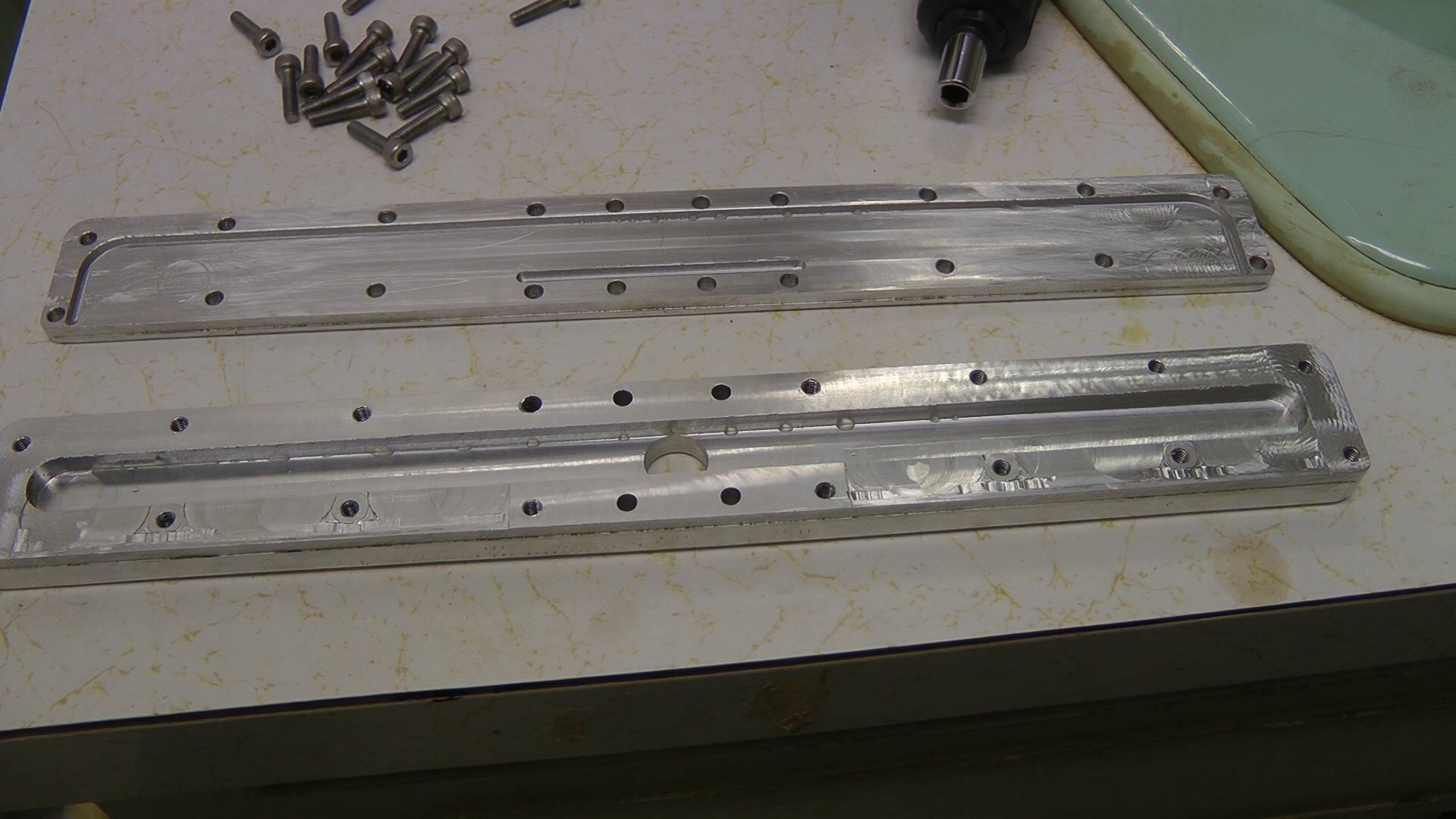
Altium Designer has powerful 3D tools, allowing you to export a STEP model of a PCB. This is very convenient as a complete 3D model of your PCB can easily be imported into CAD programs such as Solidworks.
There is a problem when doing this with with multiple different PCBs, however. Due to file naming when Solidworks imports the STEP file, each separate PCB has a model named “Board” for example that is the model of the bare PCB. Since the assemblies for each PCB have the same part named “Board”, Solidworks will use the same bare PCB model for all the assemblies, which is clearly wrong. This problem extends to other components which have the same name such as R1, C1, etc. This import procedure applies a suffix to all components to avoid this problem, allowing successful use of multiple PCBs in one assembly.
This procedure has been tested with Altium Designer 13.1.2 and Solidworks 2014 x64 SP0.0
Important: Some of these steps like restarting Solidworks may seem odd, but they must be followed EXACTLY for this to work.
For each PCB to be exported, create two folders, in this example the board is called YLM Board, so we create folders “YLM Board” and “YLM Board temp”
For each PCB, export the file from Altium (save as STEP file into the temp folder). Each board STEP file must be saved into its own temp folder, in this case “YLM Board temp”. Export using the “Prefer STEP models” option in the export dialog. (Note: the Component Suffix option here isn’t used, as it doesn’t apply the suffix to some of the parts like the bare board itself)
Open the STEP file in Solidworks, then save the Solidworks assembly in the same directory as the STEP file. A “Component documents must be saved” dialog will pop up, click Save All.
Close Solidworks completely
Open Solidworks again and open the assembly saved above. Do not skip this! I’m not sure why this is required, but the suffixes don’t get properly applied if you don’t do this.
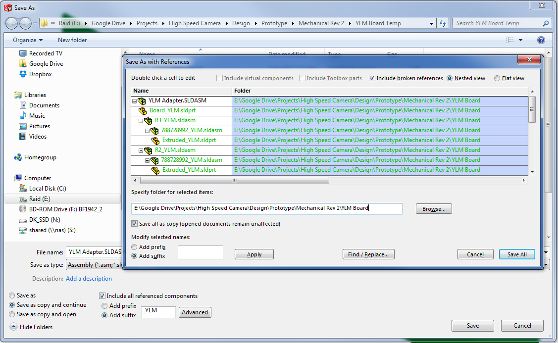
Click File | Save As. Select “Save as copy and continue” at the bottom left of the Save As dialog, check “Include all referenced components”, and select “Add suffix”. Enter your suffix in the box (in this case “_YLM”) and click Advanced.
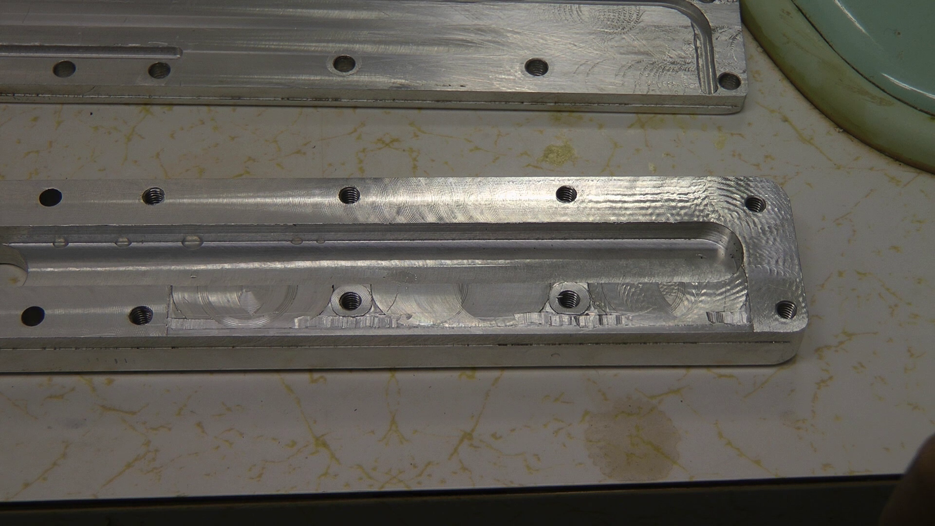
In the Advanced dialog, verify that the suffix is applied to all parts except the top level assembly (in this case YLM Adapter.SLDASM). Use Browse to select the other folder you created earlier (the non-temp one, “YLM Board” in this case). This is where the final assembly will be saved. The correct configuration is shown below:
Click Save All.
Close the assembly and repeat for other boards
Delete the temp folders
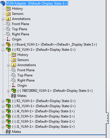
The resulting assemblies for each PCB can then be used in a single Solidworks assembly without problems. The final assembly for a single PCB is shown below, with suffixes on all components:
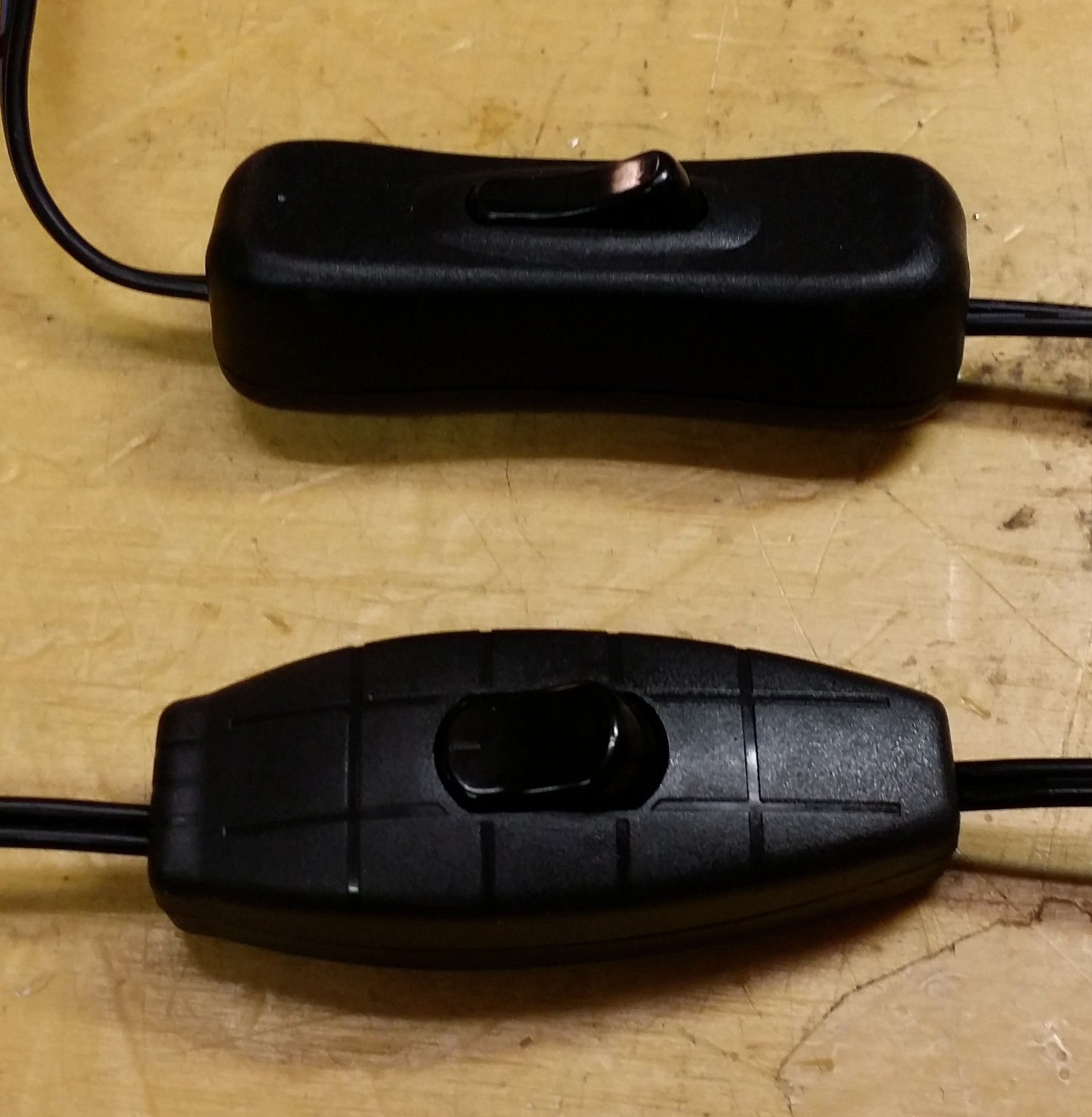
The Ikea Jansjö is my favorite desk work lamp. Some of the older ones have problems where they start flickering or stop working entirely. This is often due to bad IDC contacts in the switch. Several tutorials suggest replacing the switch as a fix, claiming the switch is not openable. Not true, you can open the switch with the right tools.
The problem appears to be mainly on the old switch design with curved sides (bottom), not the newer design (top):
Instrutions
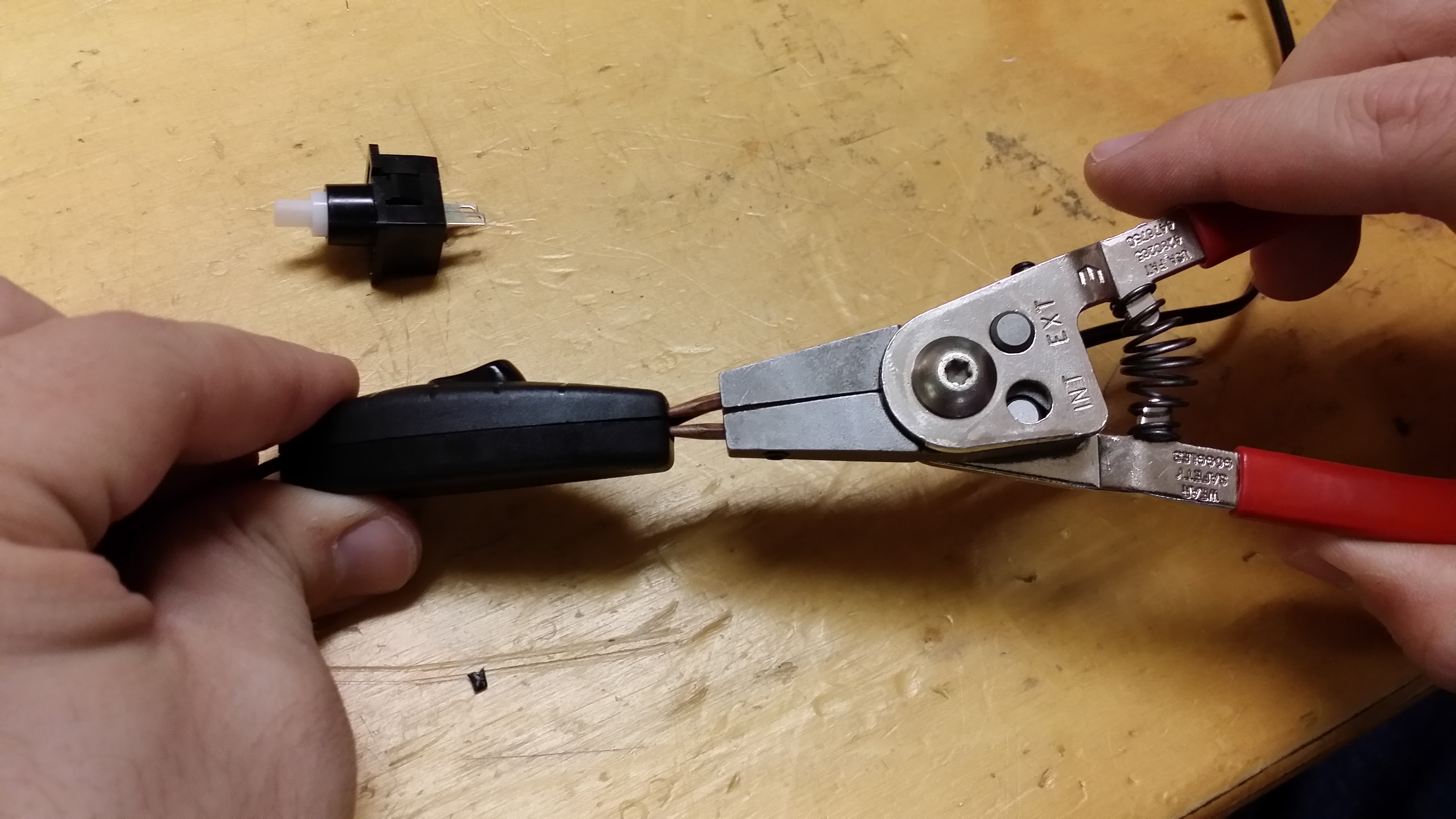
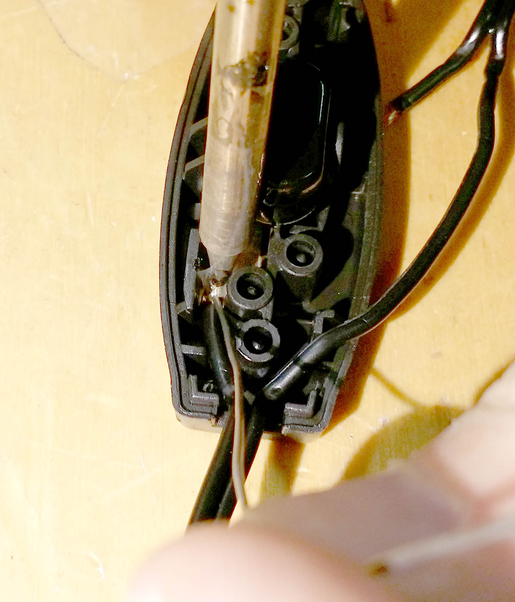
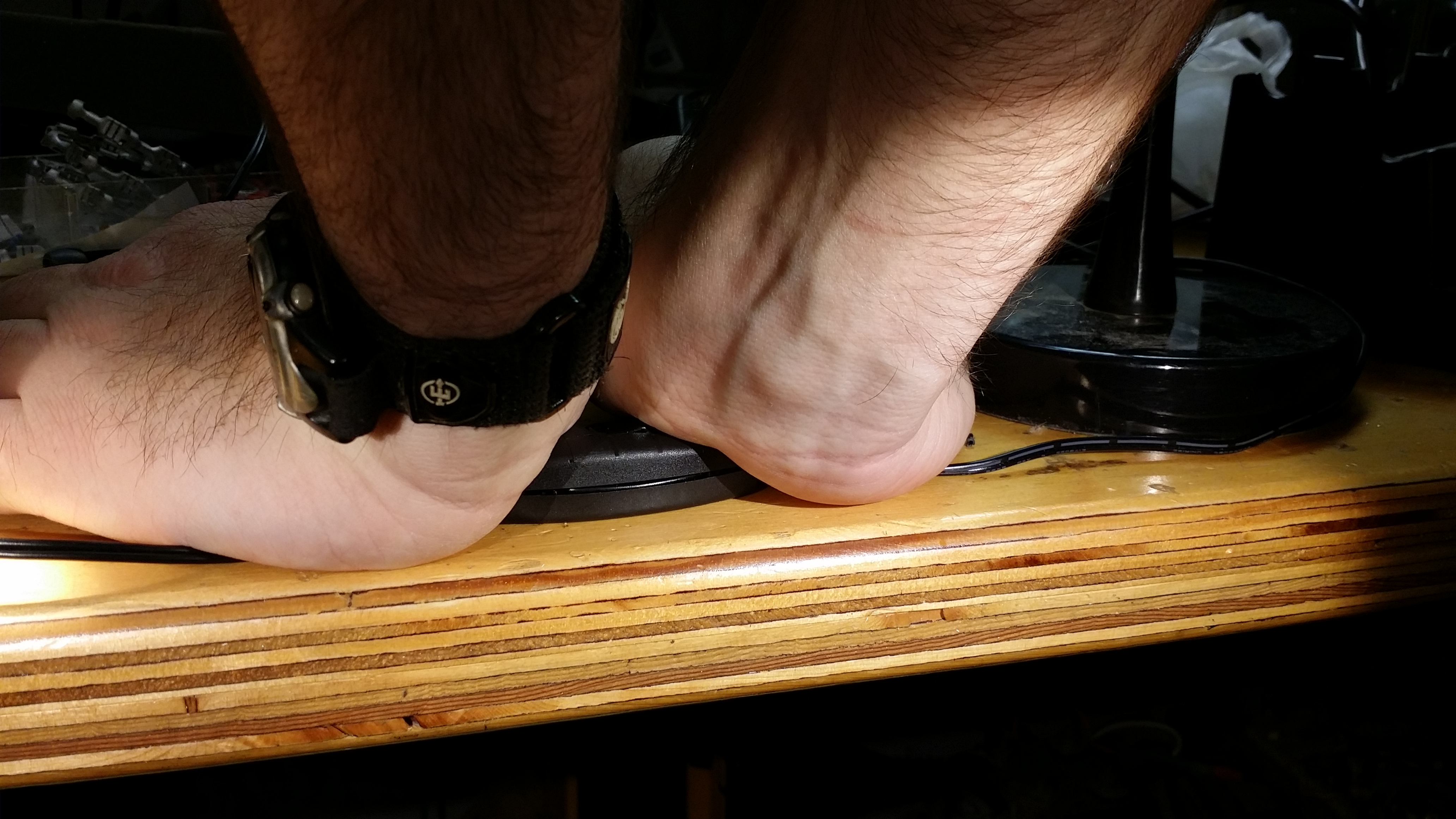
1. Open the switch
Use a pair of external snap ring pliers to open the switch. Insert them into the wire entry port and squeeze, being careful not to pinch the wire. Open one side by about 1cm, then switch to the other size to fully open the swtich. Beware of the two clear plastic strain relief pieces that may pop out from each wire entry port.
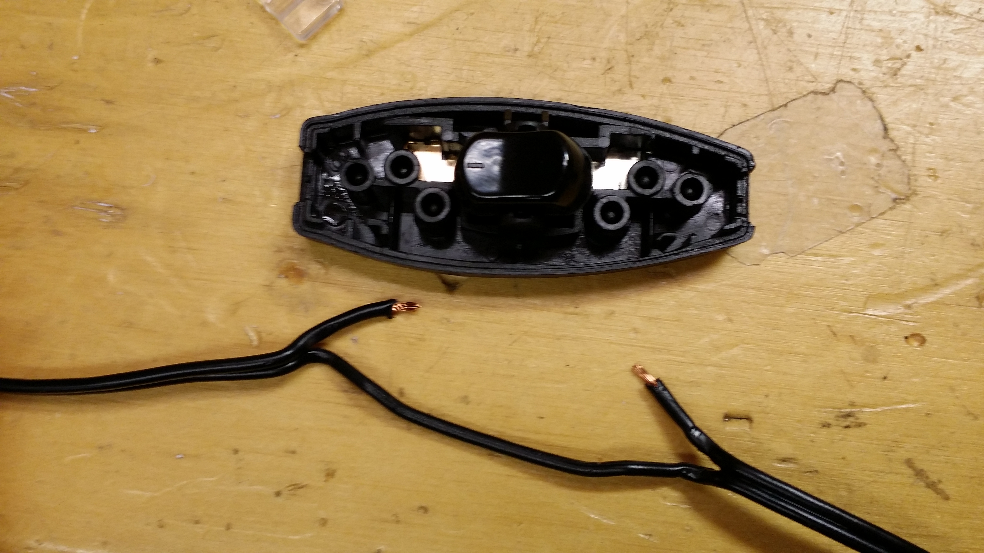
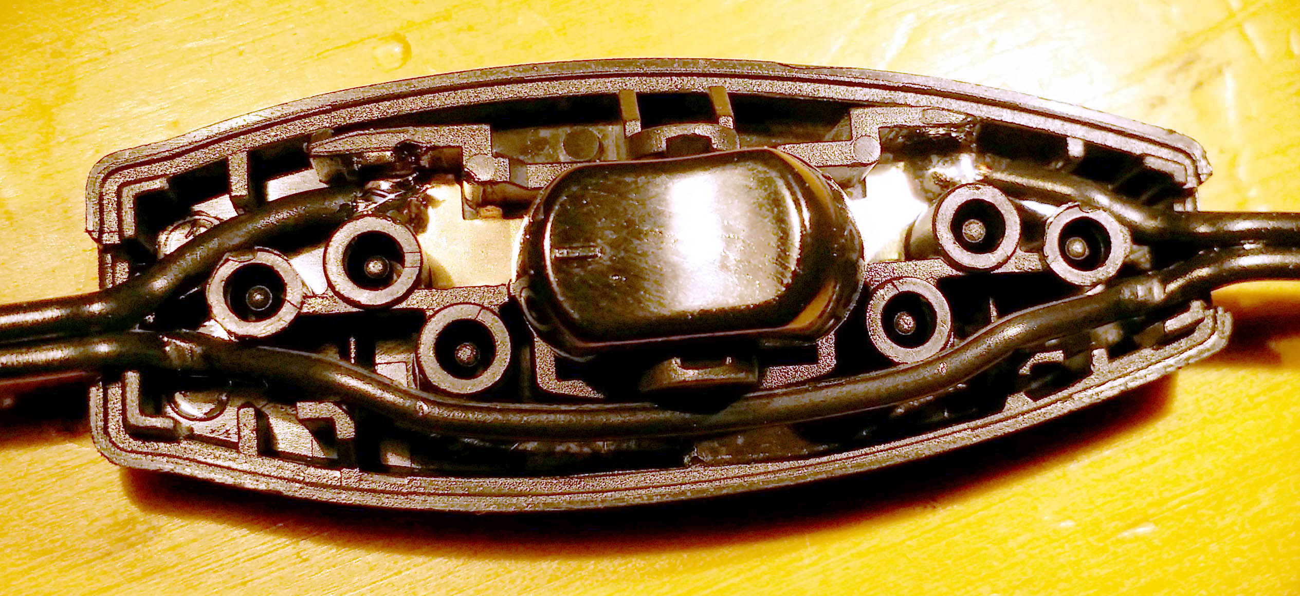
2. Prepare the wires
Carefully pull the wires out of the IDC contacts. Use a small screwdriver to hold the metal contacts down if needed to avoid pulling them out of the plastic. Strip the wires starting at the position where the contacts bit through the insulation.
3. Solder the wires in place
Use a small tip soldering iron. Place the stripped wire back in the IDC contact. You may need to push the contact open to allow it to fit.
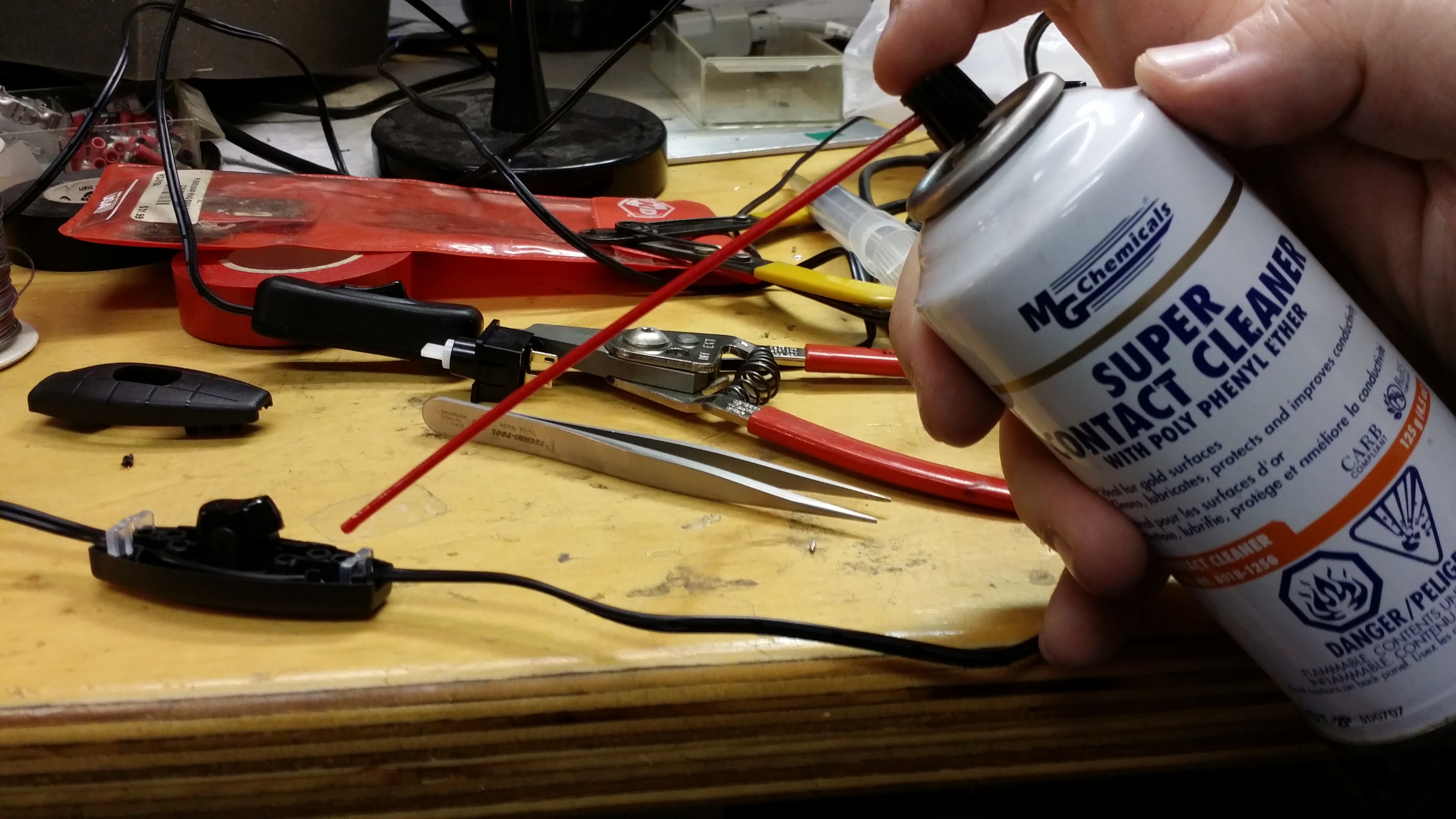
4. (Optional) apply contact protectant
Poly phenyl ether (PPE) is a super slow evaporating oil often used to protect contacts. It’s claimed to stay on for up to 40 years. This is easiest applied with a PPE-containing contact cleaner. One such product is MG Chemicals Super Contact Cleaner with PPE. Applying this may extend the life of the switch.
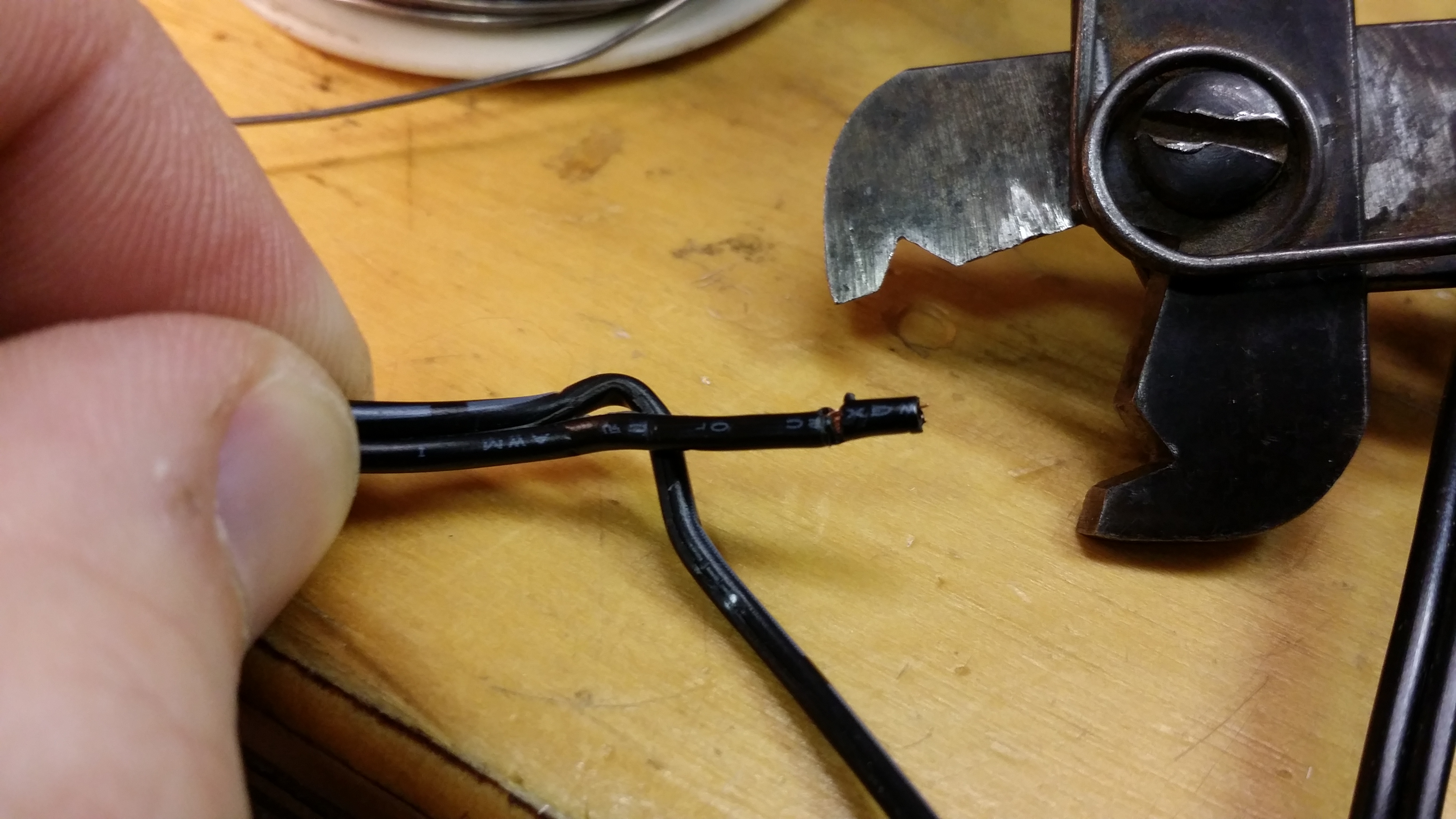
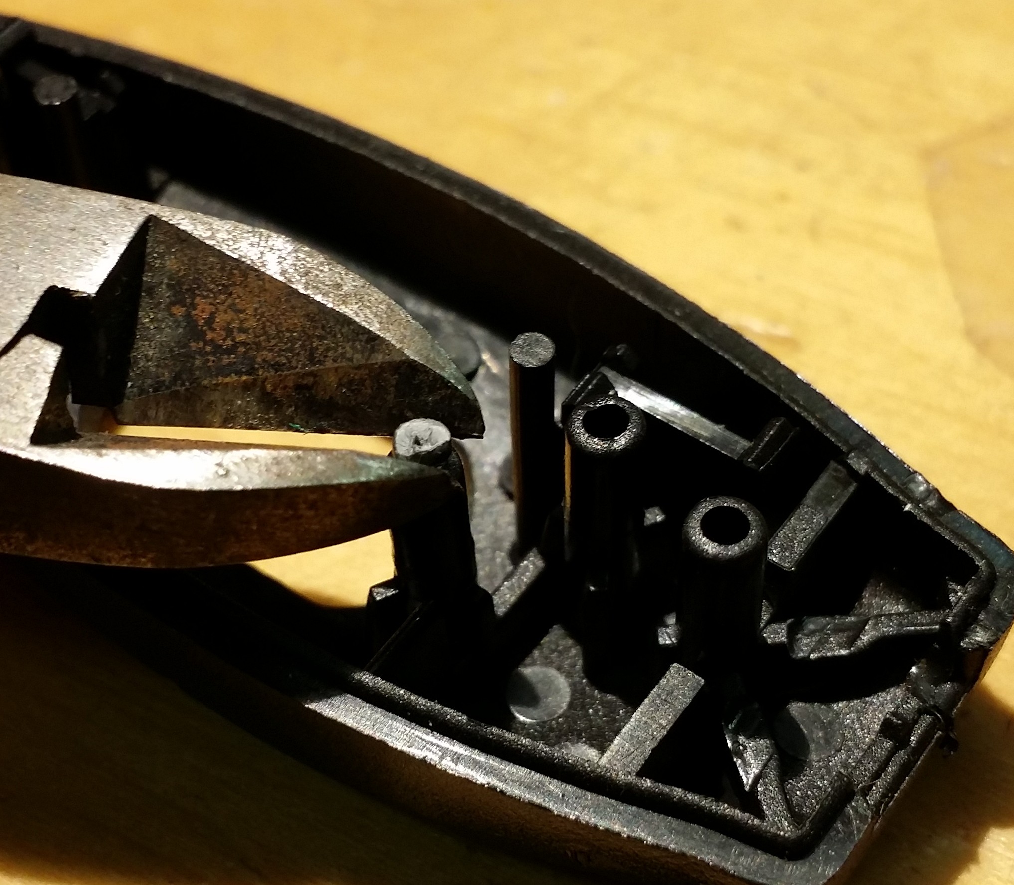
5. Cut off broken locking pins
The case is held together with friction fit pins, some of which may break off while opening the switch. Cut off any protruding nubs that are stuck on the ends of the top portion of the switch. A broken off nub is shown between the jaws of the cutter.
6. Close the switch
Place the wires back into the switch, then put the clear plastic strain reliefs back in. Place the switch on a solid table, place one palm of each hand on each side of the switch, and press down. You’ll have to push down very hard, don’t worry about the switch breaking. You may need to put all your weight into it. You may need to use pliers if you can’t push it down hard enough. Protect the switch with a cloth for example if using pliers.
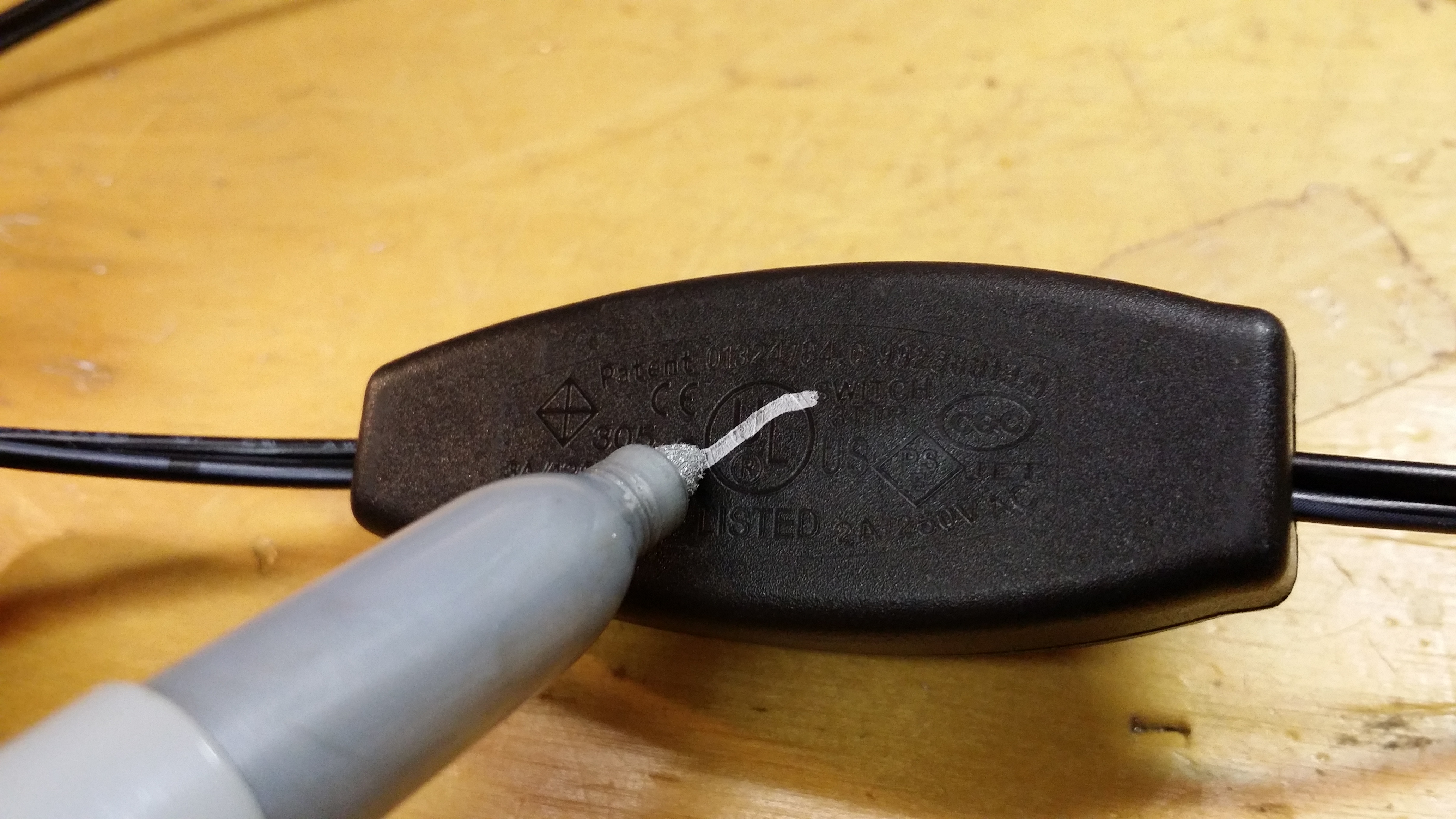
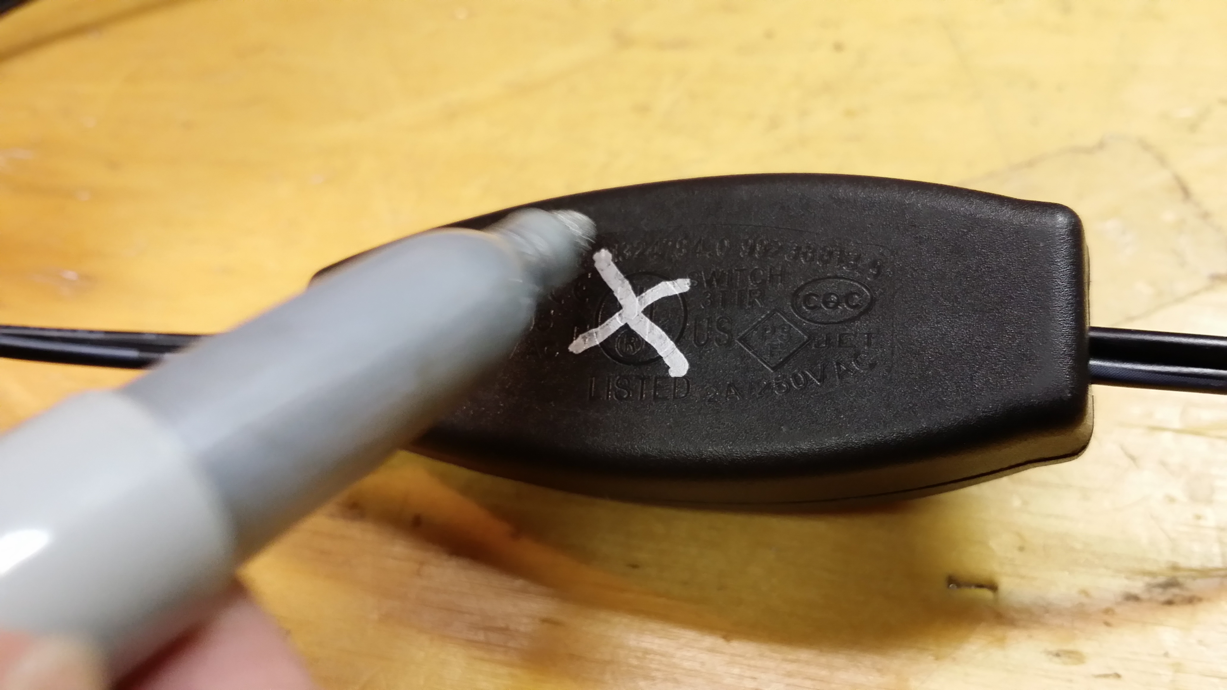
7. Do what UL should have done
This POS switch doesn’t deserve UL approval, so remedy that with a Sharpie.
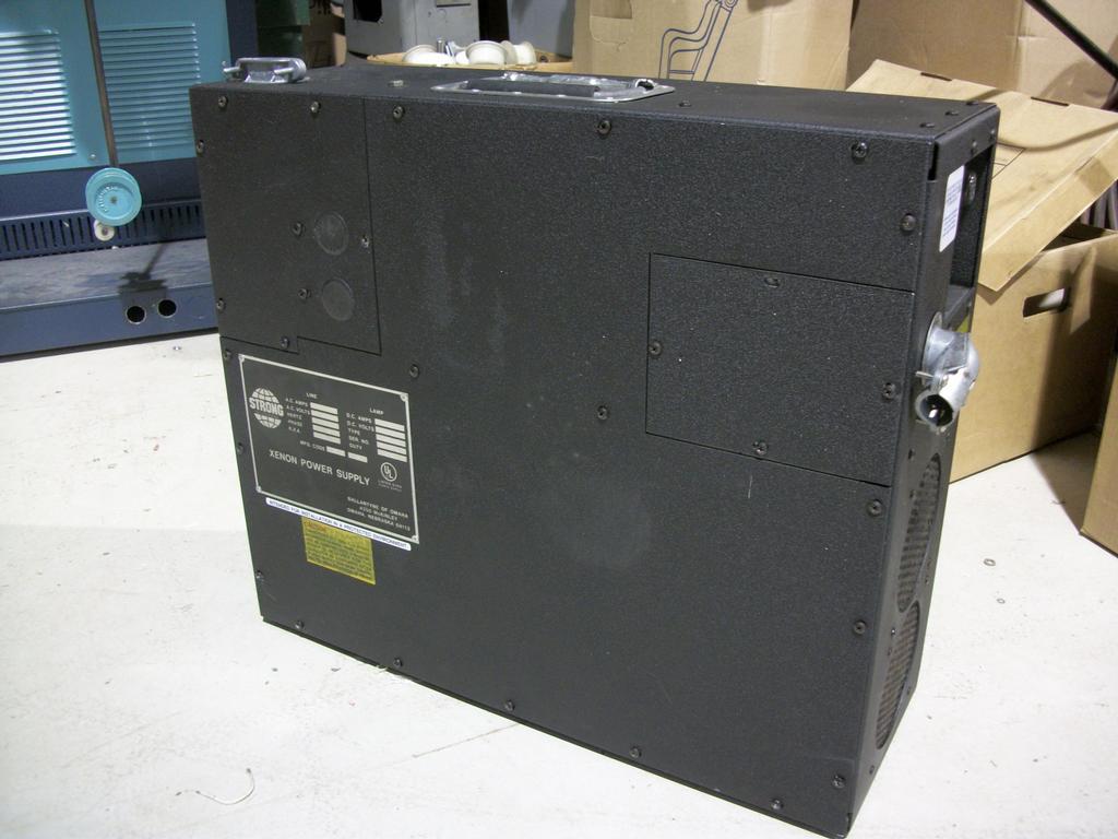
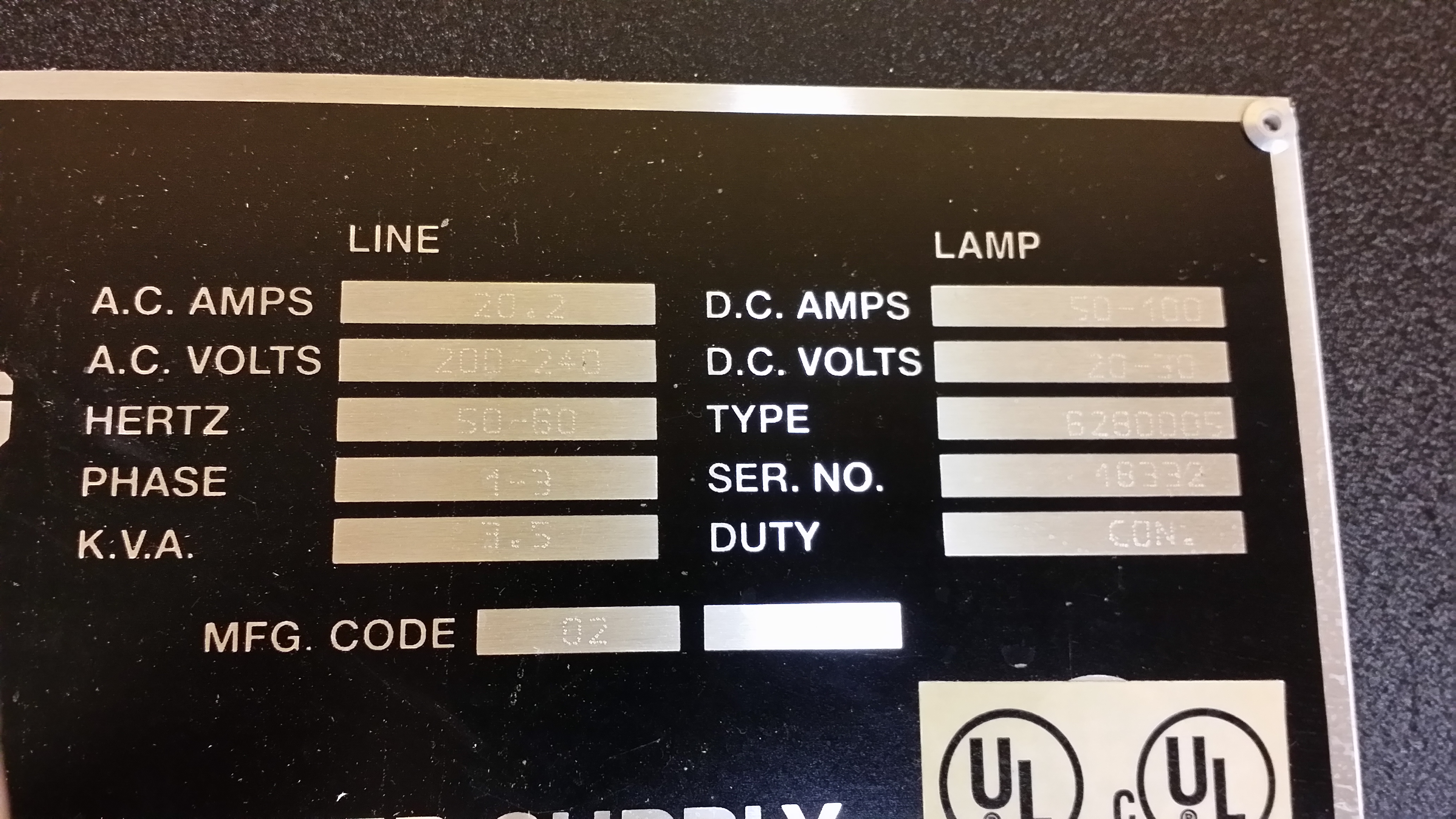
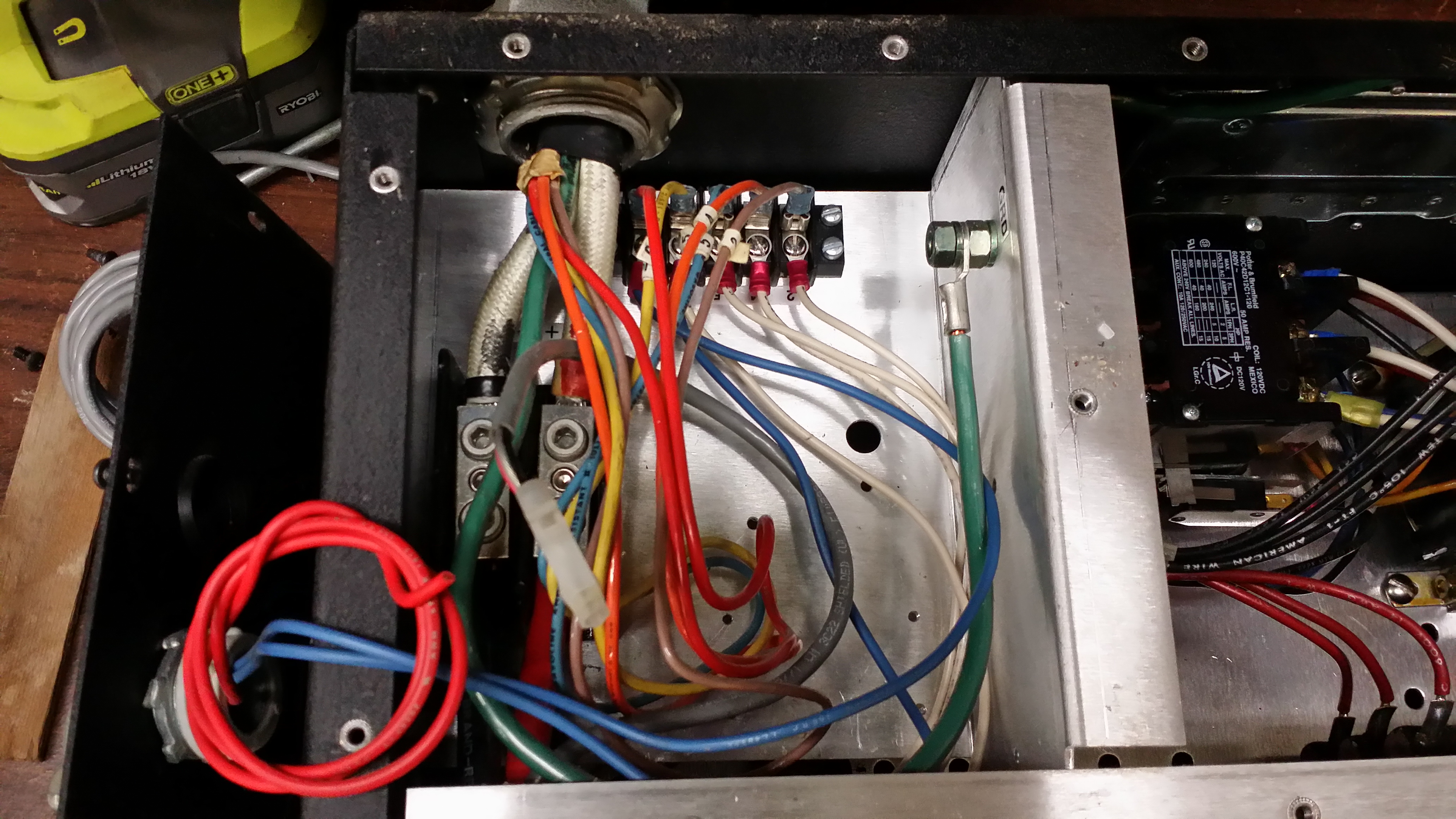
This is a Strong model 62-80005 Xenon short arc lamp ballast, out of the now demolished Station Square cinemas at Metrotown. This drove lamps up to 2.5kW for the small auditoriums in the cinema. The large auditoriums ran up to 6kW lamps.
Ratings are
200-240V 1-3 phase 20.2A input
20-30VDC 50-100A output
We were greeted with the lamp current control pot jammed in the output junction box by the installers.
This ballast dates from 1998, and appears to be an older design. As expected, it’s built very well, with the entire chassis being aluminum.
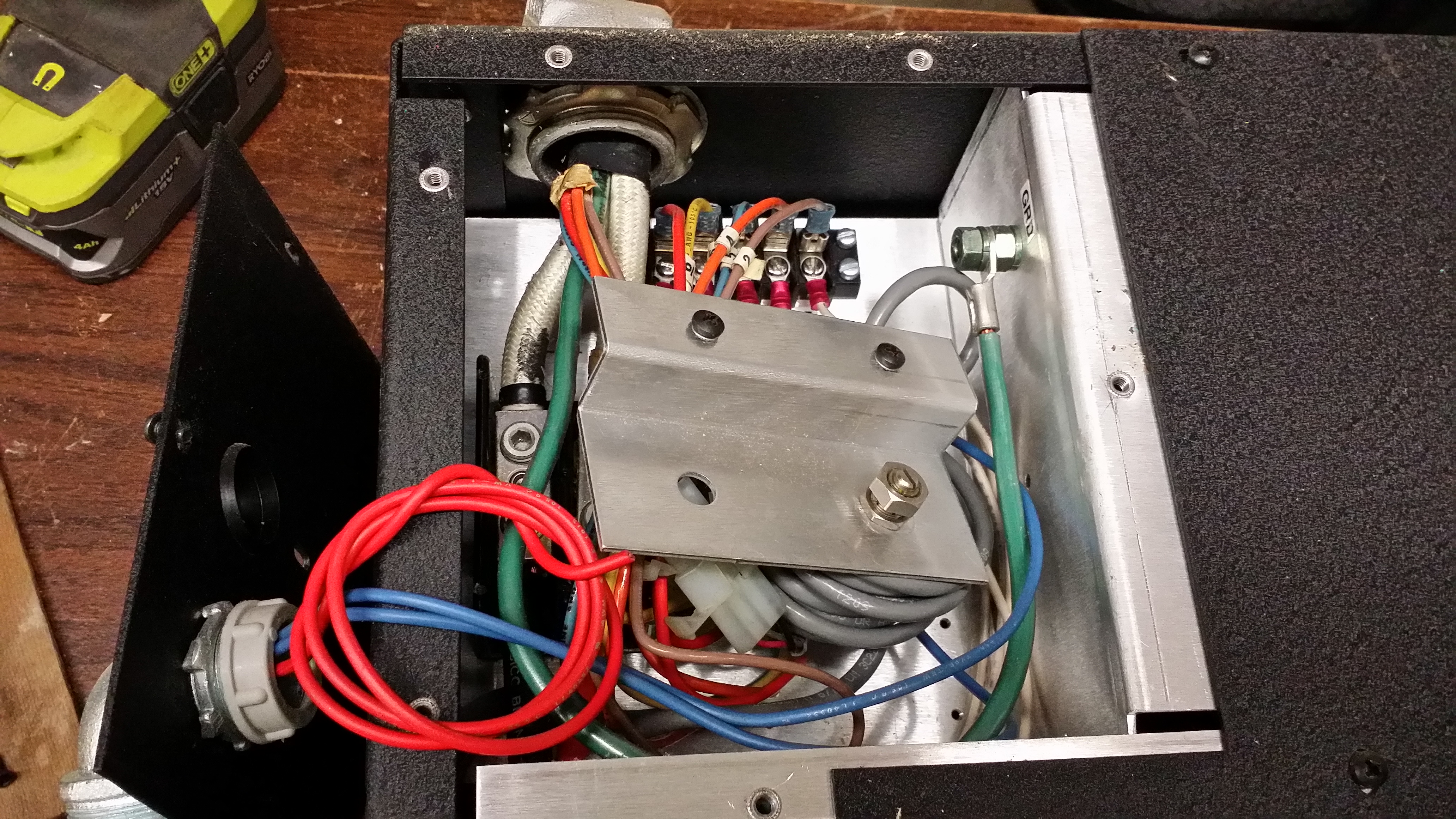
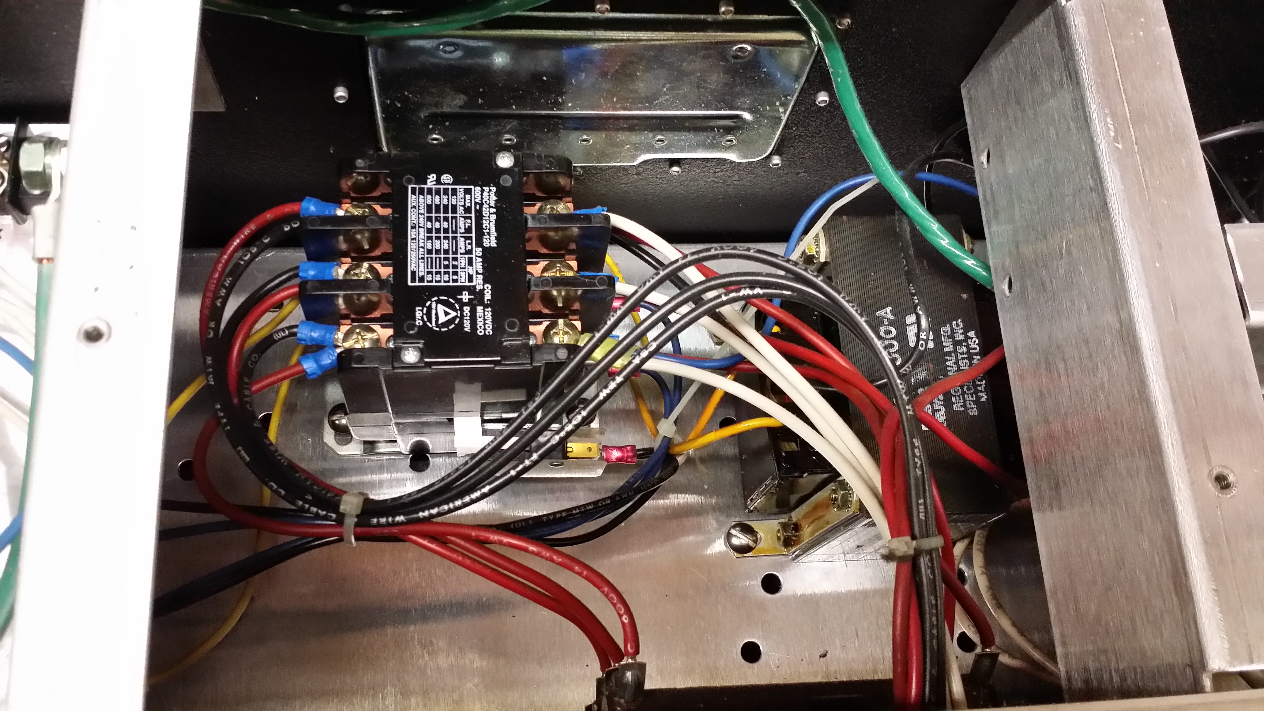
In the above photo, 3-phase input connections are on the top right, bus capacitor precharge contactor top middle, DC output top left. On the bottom right is the EMI filter and main bus capacitor (6800uF 350V), and the bottom left contains the actual switching power supply unit.
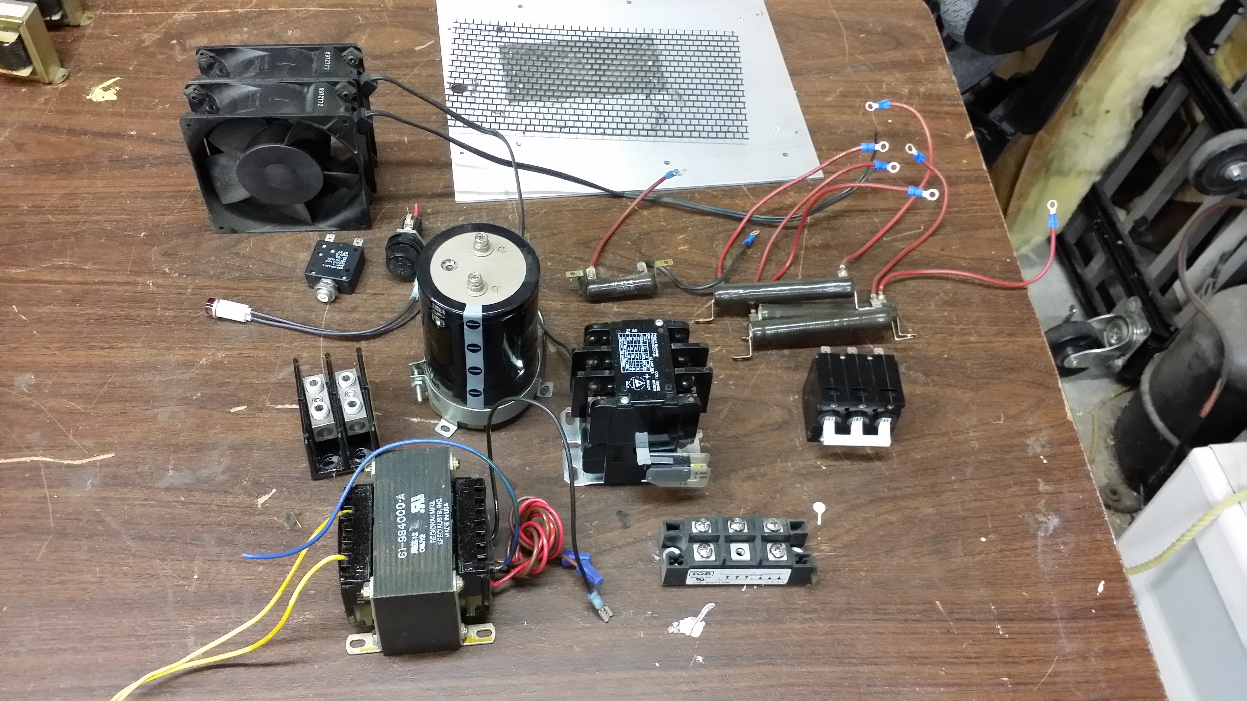
Close up of the contactor and 240-120V transformer used to run auxiliary systems in the projector. Also contains the three 5ohm 50W bus precharge resistors, which the contactor shorts out once the bus cap is charged. This avoids blowing the input breaker when turning on the power and charging up the capacitor.
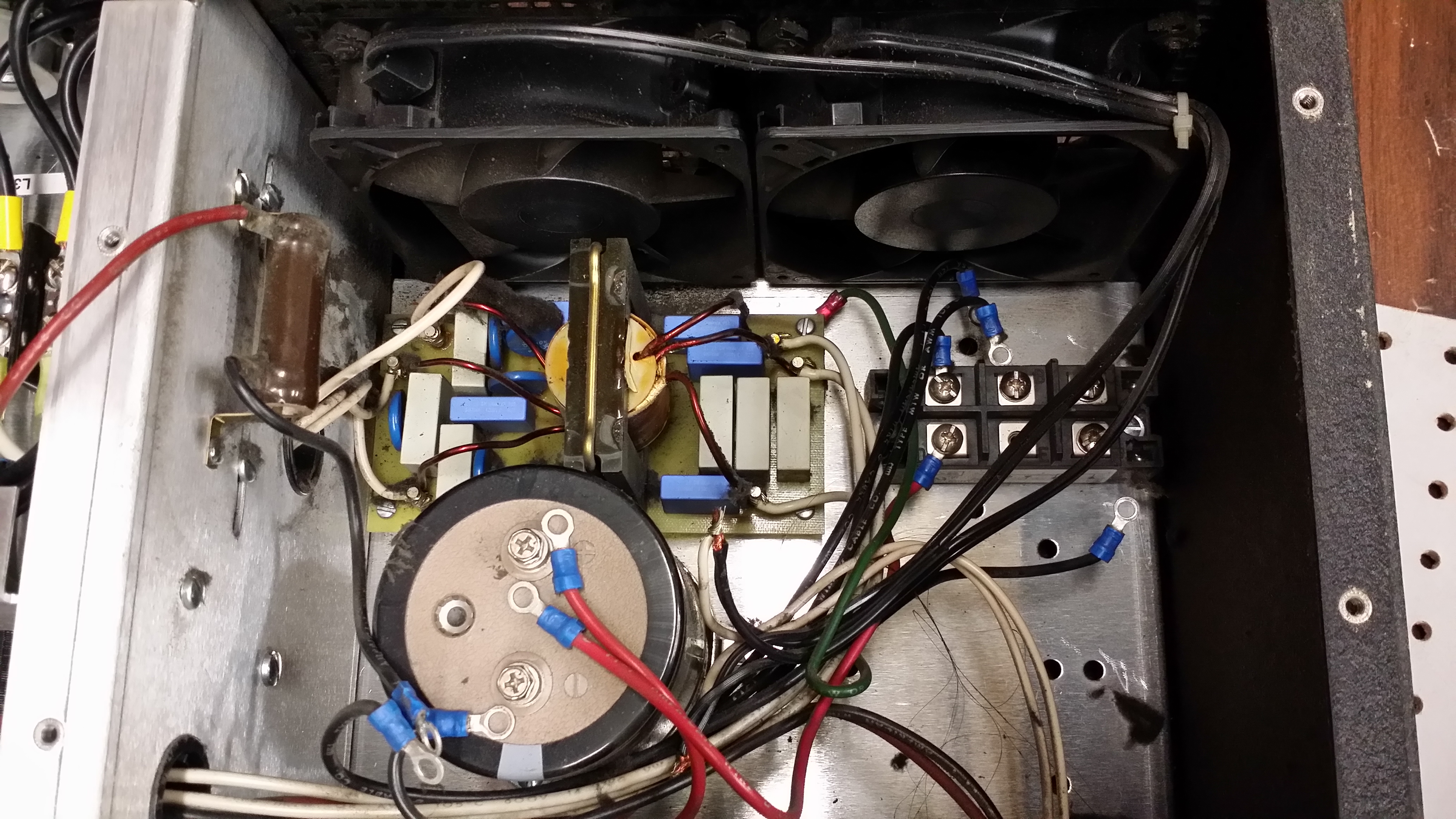
EMI filter, DC bus cap and input rectifier. Bus cap bleeder resistor also visible on the left.
DC Output terminals
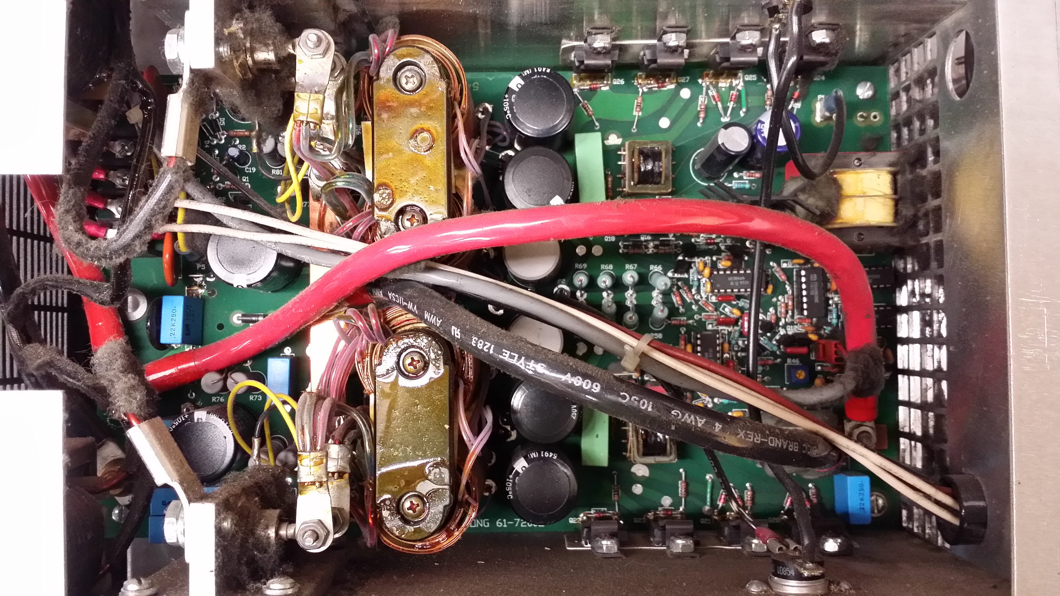
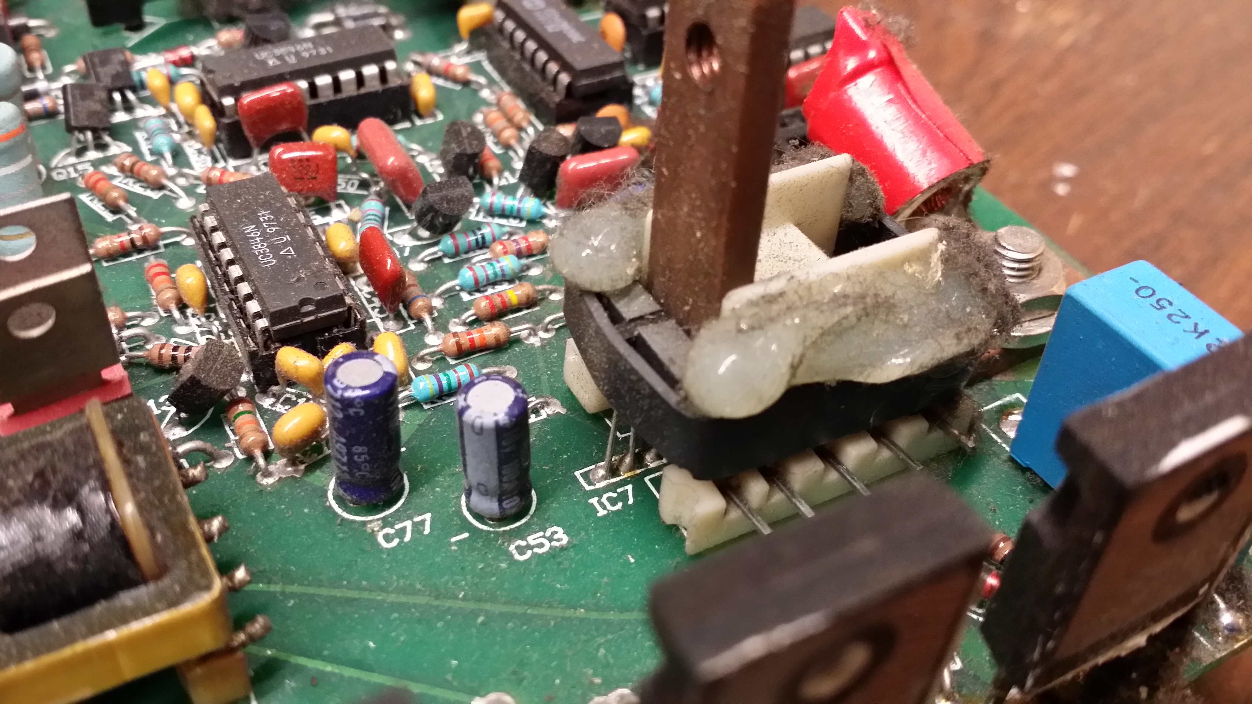
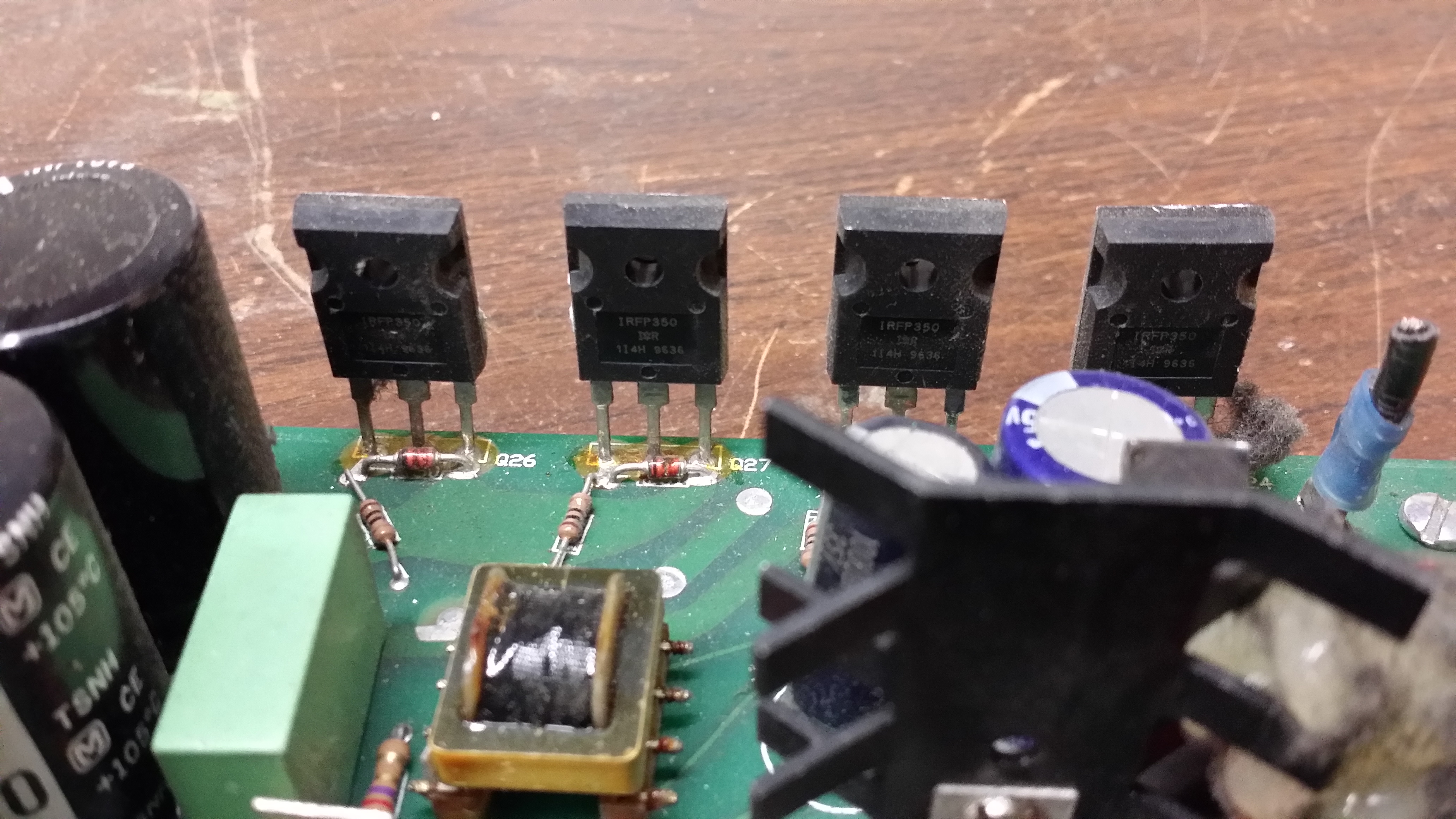
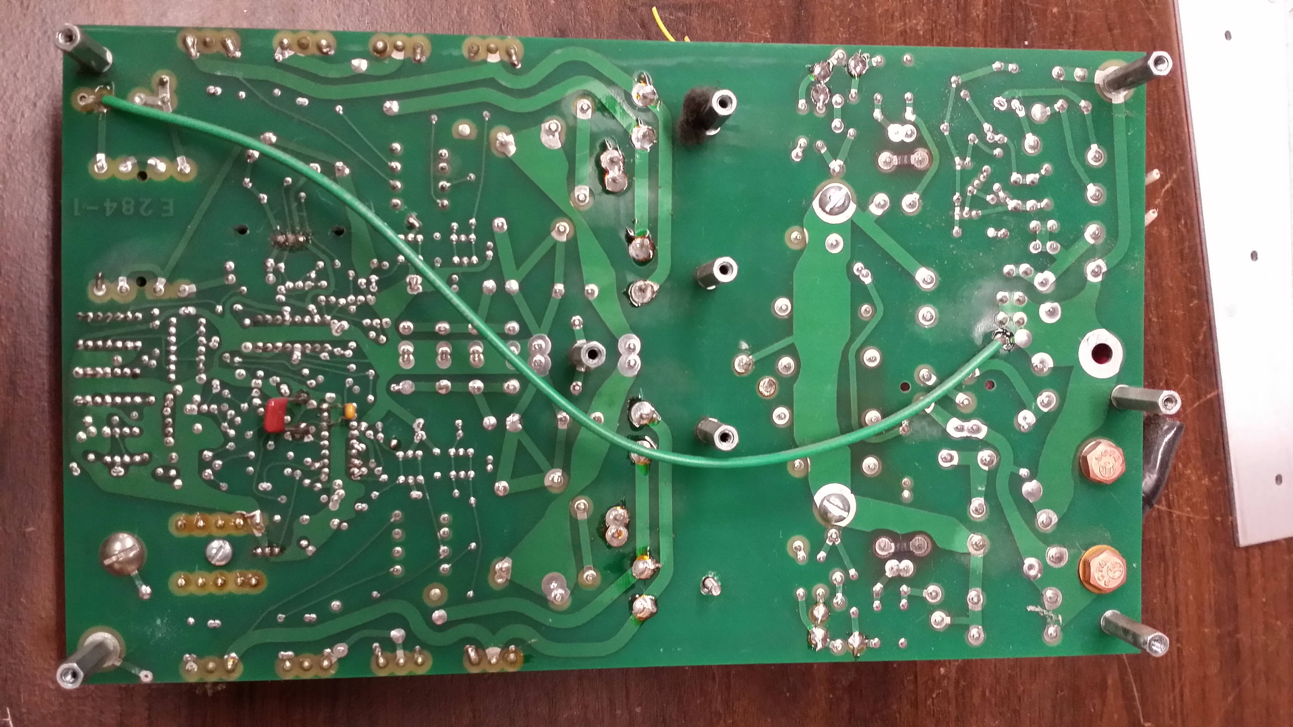
Switching power supply
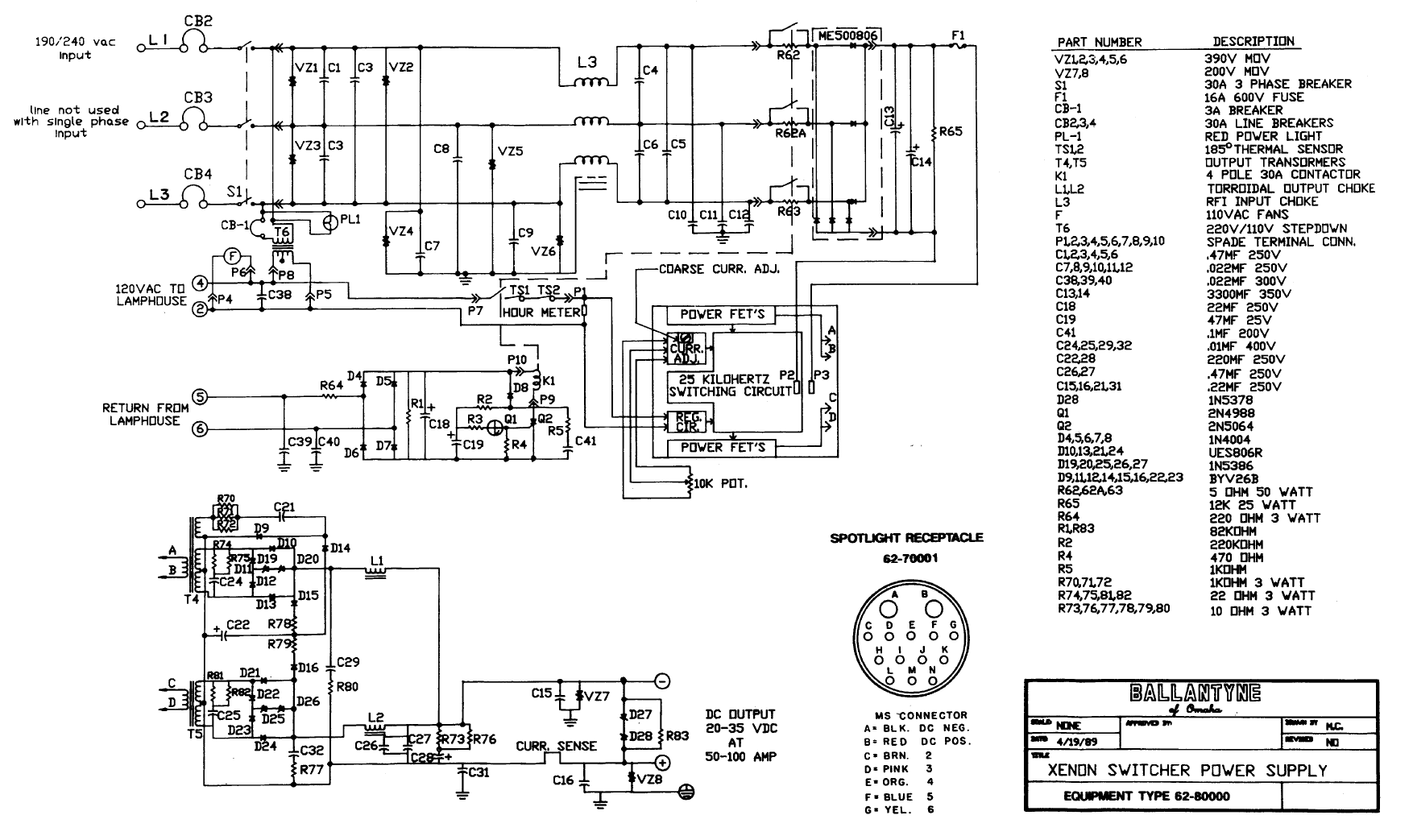
Schematic from manual. It’s basically two separate paralleled full bridge converters with full wave centertapped output rectification.
Control section has a very “organic” layout, the designer must have really been cramming to get everything to fit.
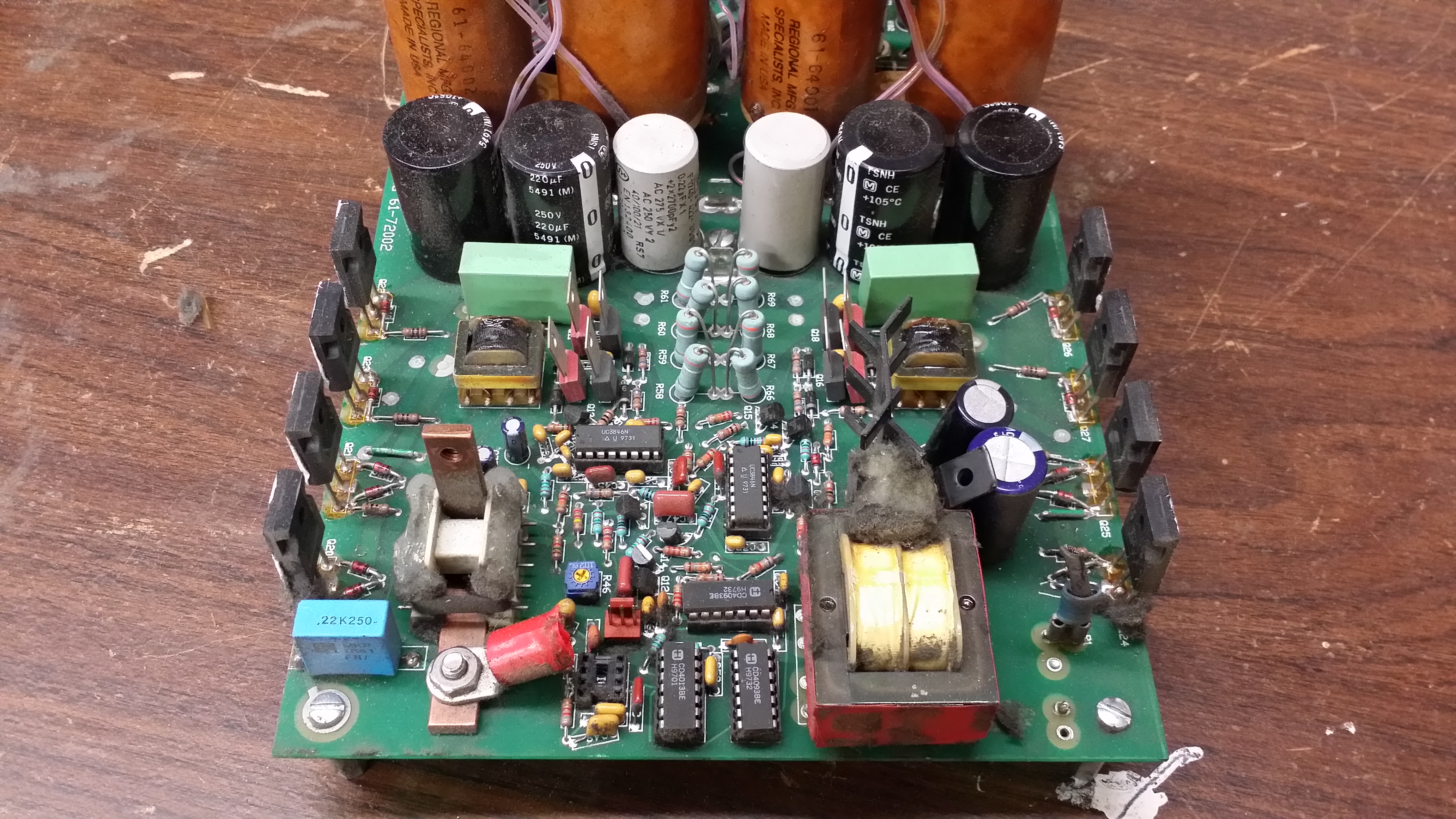
The output current sensor is clever, just a standard ferrite core with a hall sensor stuck in the core gap. Probably much cheaper than the commercial versions of these sensors, especially at this current rating.
The HSC80 was a fun project, but suffered from speed limitations, as well as a limitation facing almost all high-speed cameras: it requires a PC to fully operate and save videos. From the beginning of the HSC80 project I was intending to use the LUPA1300-2 image sensor in a camera. This sensor is about 10x faster than the HSC80’s LUPA 300, capable of 1280×1024 at 500fps as well as higher speeds at lower resolutions, beyond 2000fps at 640×480 for example.
The name HS768, like the HS80, refers to the data rate of the image sensor, which is 768Mpix/s, or about 960MB/s once the 10 bit data format is considered.
Since I didn’t have my website up when I started this project, these first few posts will be a quick overview of the progress of the project.
Design Goals
Going into this project, I wanted to create a high-speed camera that operated like any consumer camera would, as well as doing what normal high-speed cameras do. It had to:
Fit into a comfortable handheld format
Operate standalone with built-in UI – fully operable without tethering to a PC
Save video to removable media (SD card, USB, SATA drives)
Save to compressed formats directly using modern compression (h264) as well as uncompressed formats
Be controllable remotely via Ethernet, as these cameras are sometimes used near things you don’t want to be near (exploding things, flying debris, etc)
Build for less than $3k parts per camera
Design
Originally the entire system was going to be built into an FPGA, and this is how I built the initial prototype:
I quickly realized the software would be a massive project. Supporting various filesystems for removable media (FAT, NTFS (because who likes 4GB file size limits?), EXT3) would be a massive and time consuming software challenge. Implementing h264 compression in an FPGA is also a formidable challenge unless you buy an off-the-shelf IP core, and the performance is limited in low-end FPGAs.
The solution to these problems is simple. Let someone else do all the hard work!
How do you do that (without paying someone)? Take advantage of open source, running Linux on top of a SOC (system-on-chip) video processing IC, something that would typically be used in digital video recorders, security systems, cameras, etc. Linux takes care of the pesky details of storage support, and the SOC and associated drivers provide hardware h264 encoding as well as support for all the Linux niceties without having to write drivers.
As a side benefit, adding a SOC actually reduces the system cost, because FPGA space very expensive compared to an ASIC, so the smaller FPGA more than makes up for the added cost of the SOC.
Enter Davinci
SOCs are notoriously “protected” by their manufacturers, case in point the Raspberry Pi. The Pi’s SOC datasheets are only available from the manufacturer under NDA, and they usually won’t even talk to you unless you’re purchasing huge quantities of parts. The parts usually have short lifespans, for example SOCs used in phones may remain in production for a year or less. There are a few exceptions to this rule, mainly some parts released by TI and Freescale. The industrial segment of the market usually has longer production lifetimes, with TI claiming that they will not obsolete a part if anyone orders it within 3 years. That claim should probably be taken with a grain of salt however.
The speed at which you can save video is limited by the speed of the memory card or video compression, so the faster the better. At the time of selection, the fastest single channel h264 compression in an industrial part was the DM814x series from TI’s Davinci line. The DM8148 supports 1080p60 compression in real time, and has other nice features like a 1GHz CPU (ARM, not that architecture really matters), USB host, SATA, HDMI, multiple video ports, etc. Just the ticket! Software support is provided with a TI Linux branch with all their drivers built in.
DDR3 woes
High speed cameras usually store data to a RAM buffer due to the high data rate, although some manufacturers offer ludicrously expensive custom SSDs that allow shooting at partial rates for long durations. DDR3 RAM is the logical choice as it’s abundant and cheap, especially in DIMM/SODIMM format. Unfortunately most FPGAs only support components (RAM chips mounted directly on the board), not full modules. Due to the consumer market for modules, ordering a single chip can cost almost as much as an entire module which could contain 8 or 16 chips, so there’s serious pressure to use modules.
Neither Altera nor Xilinx support DDR3 modules in an FPGA costing less than $1k. One manufacturer, Lattice, does offer DDR3 DIMM/SODIMM support in their ECP3 series, and this was the driving force in selecting the ECP3 for the camera.
Archetecture
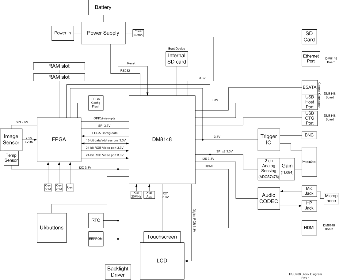
The camera is basically split into two sections. An FPGA handles data acquisition from the image sensor, storing the data into 16GB of DDR3 RAM, allowing about 20s of record time at full speed. The FPGA converts the raw sensor video into a fully processed RGB video stream which is sent to the DM8148.
The DM8148 takes care of saving the video stream, and controls the whole system, proving all the niceties you get on a modern PC: Graphics, HDMI, USB, SATA, SD cards, etc.
Board Layout
I didn’t document the layout process in great detail, but I did get a nice timelapse of the DDR3 memory layout for the DM8148:
DDR3 Routing Part 1
DDR3 Routing Part 2
And here are the current prototype boards finished:
Installing a central compressed air system begged the question “What useful things can we do with compressed air?” One of the first ideas was to make a clone of the Dyson Airblade type hand dryers for the bathroom, to eliminate those dirty shop hand towels.
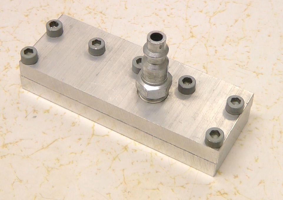
The basic concept is to have two flat air nozzles aimed at each other, replicating the Dyson, except supplied by compressed air rather than a vacuum cleaner type blower. The first prototype was made on the manual mill, out of 1cm aluminum bar, and simply plugged into an air line. It only provided one out of four required nozzles, but running it over a wet hand proved the principle.
It also generates enough thrust to hover nicely!
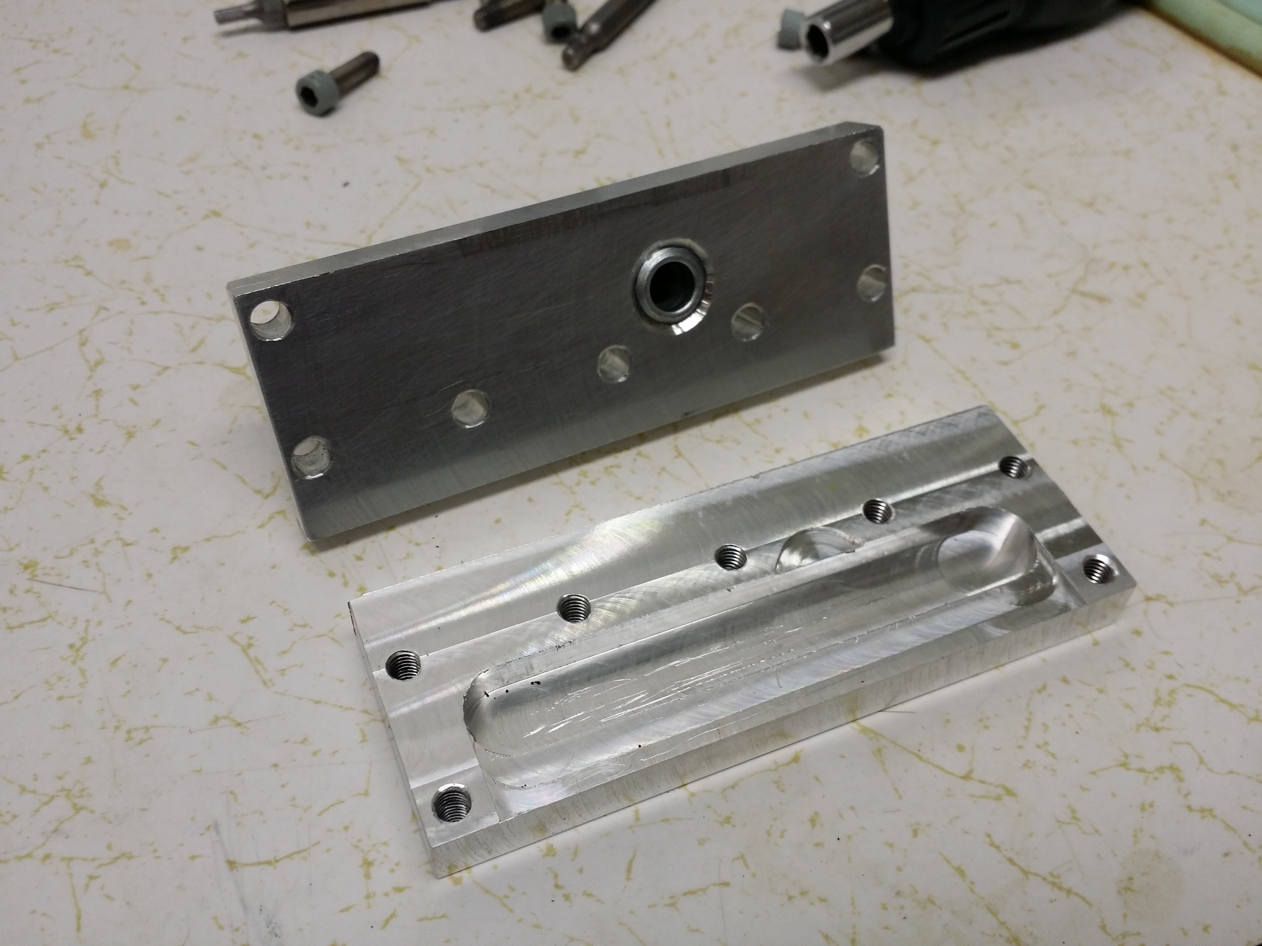
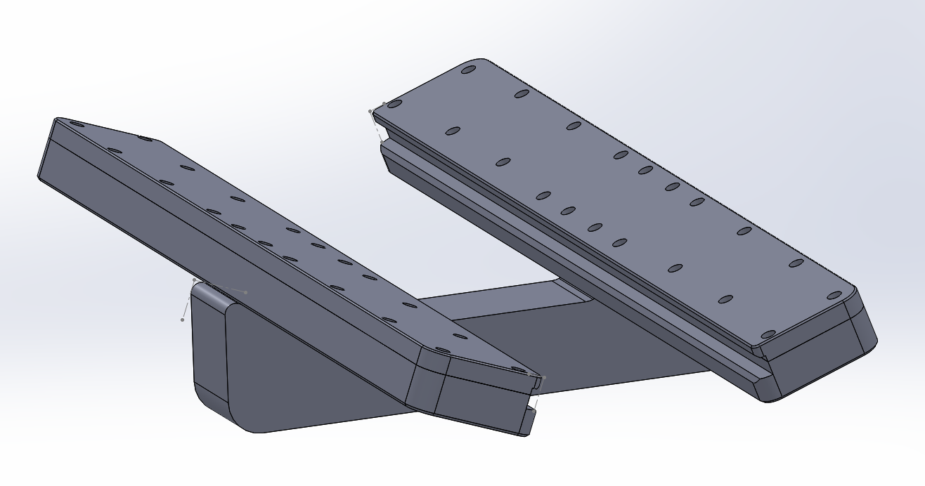
The concept proven, the entire dryer was modeled in Solidworks. The width of the air nozzles and hand space between the nozzles was selected based on the size of a typical hand, Small protrusions were added in an attempt to keep the skin from getting too close to the high velocity air near the nozzles, but these caused the air to “stick” to them and go straight down or straight up, and had to be removed later.
Airblade Solidworks Model These models need to be updated with the new air nozzle gap of 50um as well as have the protrusions in front of the nozzle removed or modified.
This was one of the first projects I did on the new Tree Journeyman 325 CNC machine. I did a timelapse of the machining process.
Initially the air nozzle gap was machined at 25um, but this turned out to be too small, and resulted in inconsistent airflow over the width of the nozzle, likely due to slight variations in the cutter height over the width of the gap. This was then increased to 100um, which appeared to work well while testing the dryer on the shop air supply with normal compressed air fittings. The dryer was then installed onto the wall.
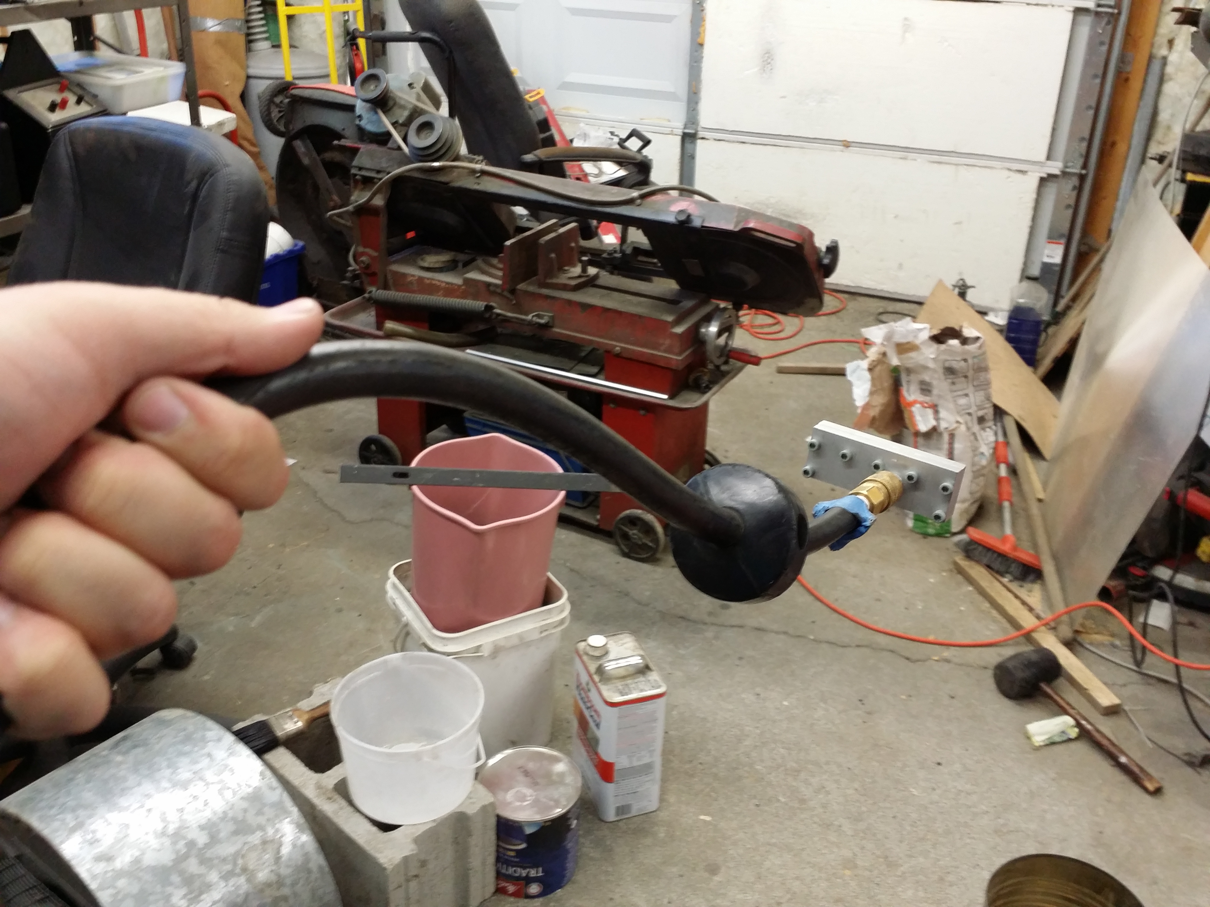
Initially a foot operated pneumatic valve was tried, but was found to be far to restrictive to airflow, resulting in almost no output. Proper valves that pass enough air were found to be far too expensive, so a 3/8″ solenoid valve was installed, which solved the airflow problem.
With the dedicated air supply line and free flowing solenoid valve, the dryer was found to be far too powerful and was unpleasantly loud compared to earlier testing. The restriction of the typical M connector used on the shop air line was significantly reducing the pressure to the dryer. More experimentation and re-machining the prototype unit showed that an air gap of 50um was appropriate, and this modification was made on the dryer, as well as the installation of an adjustment valve shown on the air line feeding the dryer.
The dryer is as effective, if not more so, than the Dyson Airblade thanks to the very strong airflow provided by shop air pressure. Sound is comparable with the adjustment valve set to a level that approximates the effectiveness of the Dyson. With the valve up all the way, drying is significantly better than the Dyson at the expense of noise. Air consumption does not seem to vary much, as higher flow rates allow you to move your hands through and complete drying faster which compensates for the higher airflow rate. This unit is also far cheaper, costing only about $50 in materials compared to ~$1.2k for a Dyson Airblade.
One issue left to be addressed is ensuring safety with high pressure air near skin. An open skin wound could allow a jet of compressed air under the skin with unpleasant results. The solution is to keep the hands from contacting the nozzle directly. An attempt was made with simple protrusions from the nozzles but these caused problems with airflow. The final solution is likely a wire mesh screen of some sort.
If there’s enough interest in this project, I could do a Kickstarter and make a small run of them. Let me know!
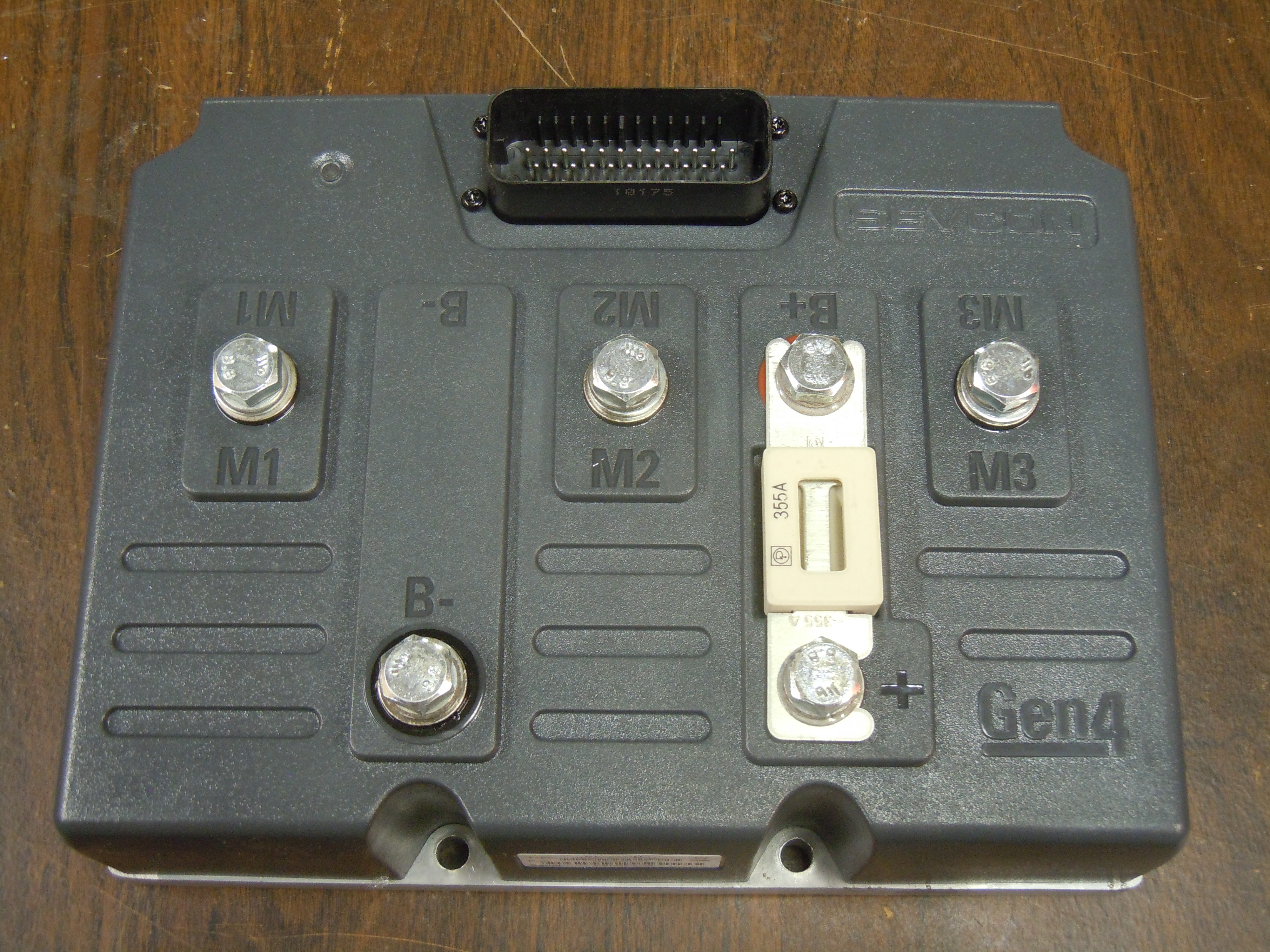
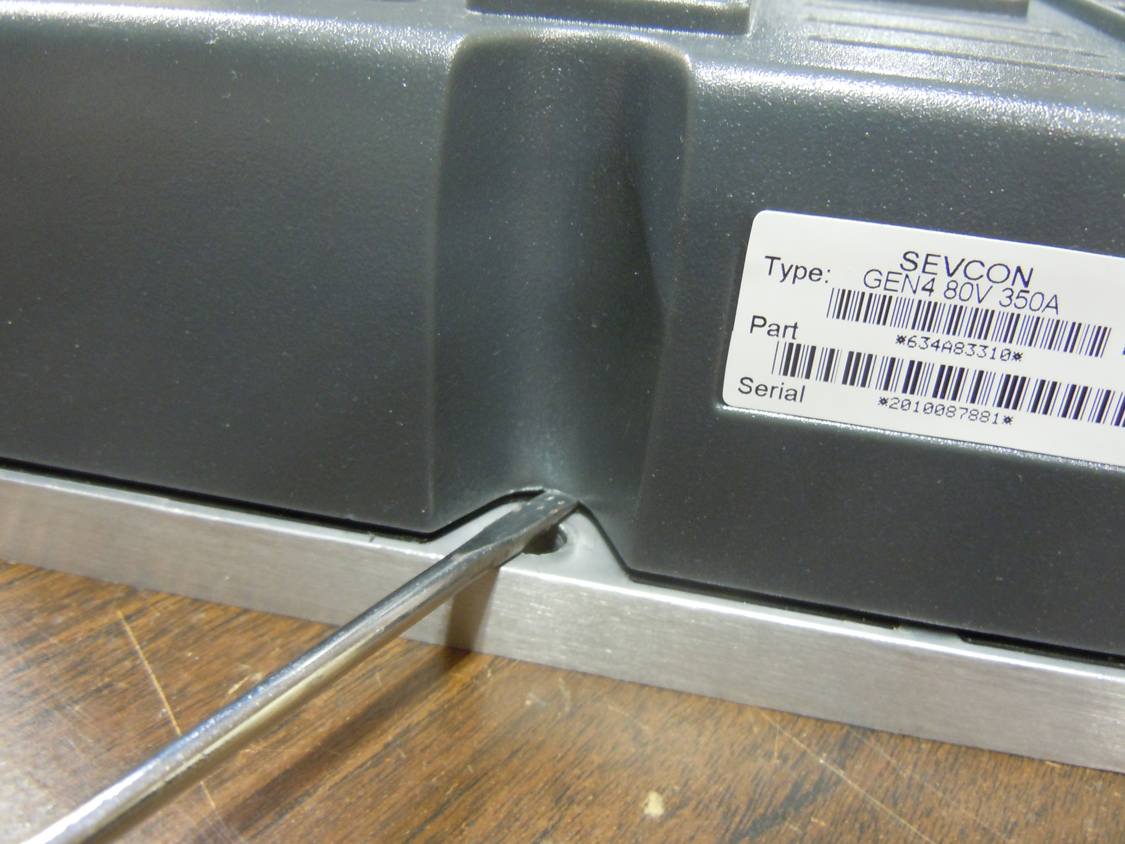
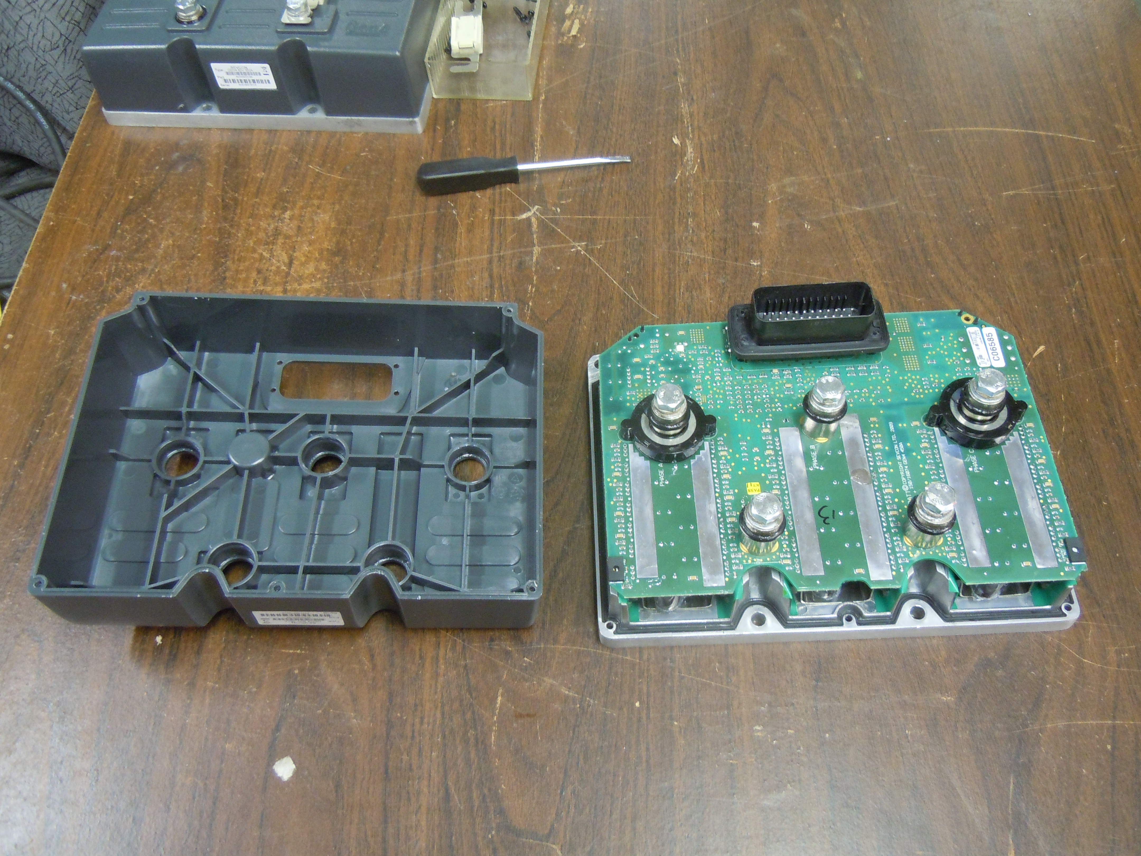
Here’s a look inside a Sevcon Generation 4 AC motor controller. This particular one is the 80V 350A model, sourced for the ArcWolf racing go-kart. Two were purchased from an eBay seller in located in Korea for US$720 total including shipping.
The controller is waterproof with a plastic shell over an aluminum base plate. Terminals protrude through the top.
With the screws removed, the top comes off with prying.
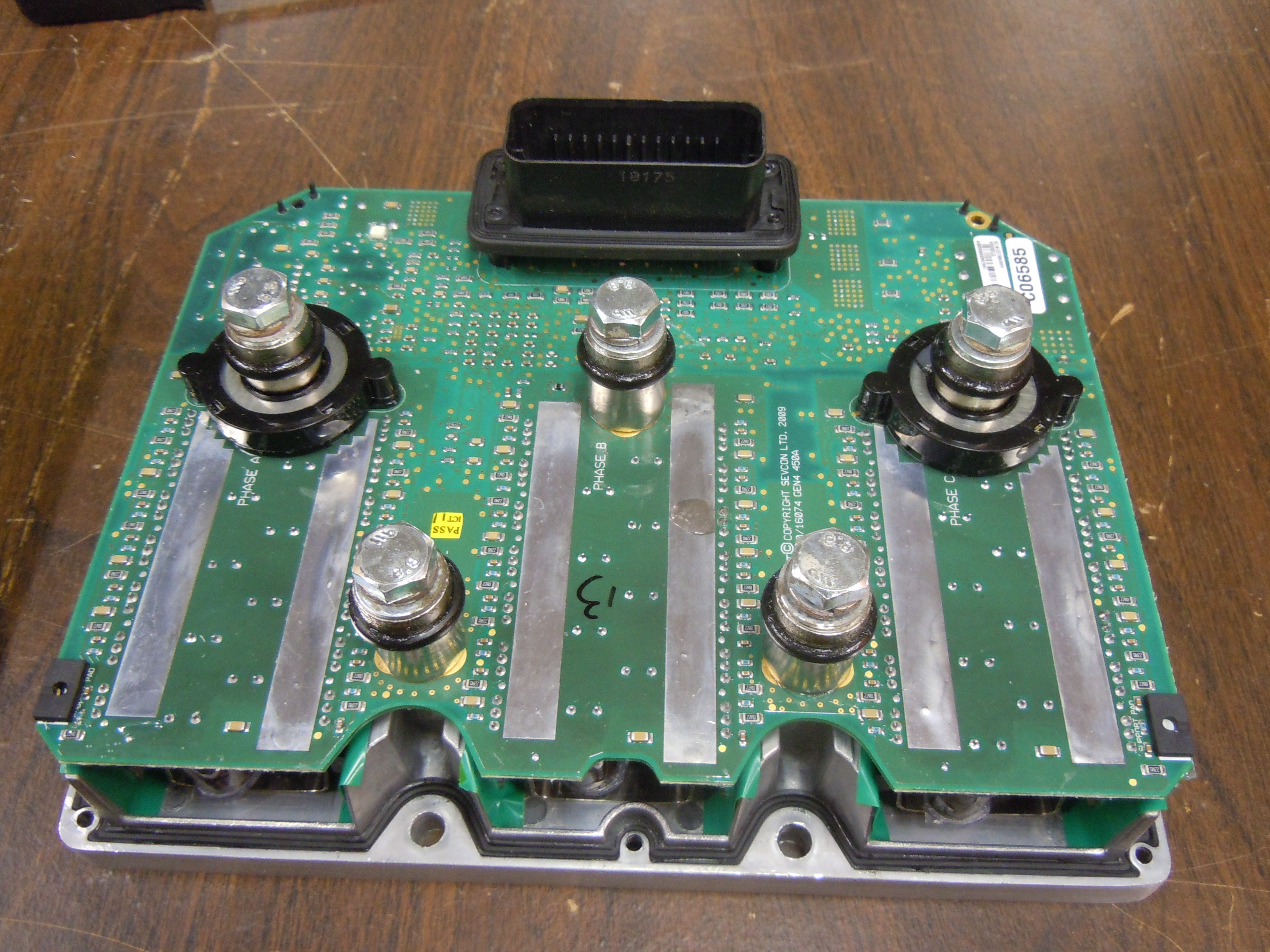
Just one big board. Surprisingly there are no bus bars, the 350A connections go directly to the PCB! The three half bridges are clearly visible. Each leg uses seven IPP075N15N3 G 150V 7.5mOhm FETs.
The PCB is at least four layer. The top and bottom layers both carry the current from the FETs to the 3 phase outputs, with the DC bus running on inner layers. The number of inner layers is not known.
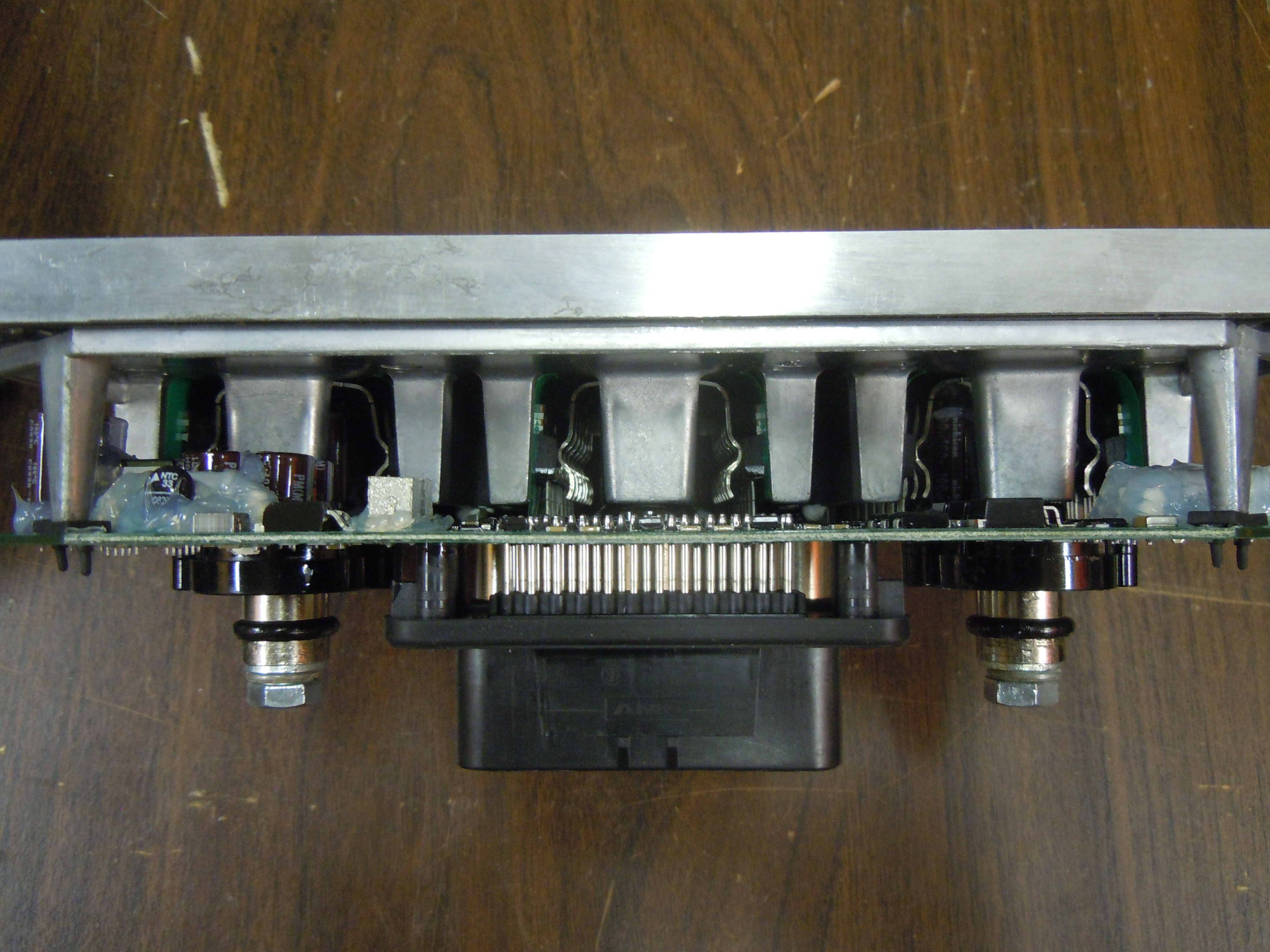
The FETs are clamped to the heatsink by spring clamps. These must be held open with a special jig during assembly while the top board is inserted.
A green thermal interface material couples heat to the heatsink. The material is basically a think Kapton sheet with a phase change material that melts at high temperature. I recall using this material in an AC inverter I built years ago because it was the highest performance economical material available. It likely still is to this day.
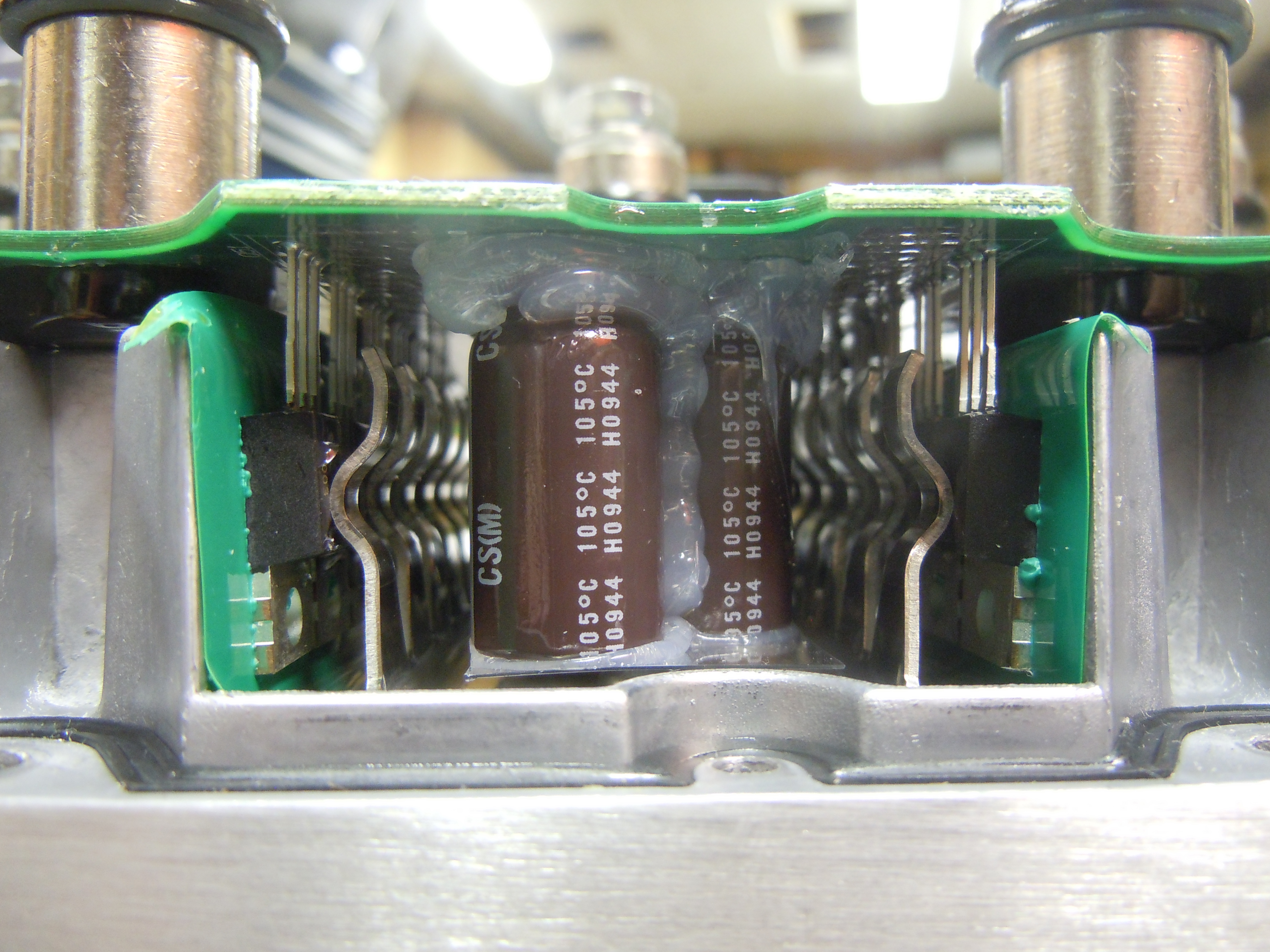
The bus capacitors are Nichicon 160V 100uF with 8 per leg (2400uF total). The capacitors and other weak components are secured with silicone to stop them from breaking off due to vibration.
Current sensing is accomplished with hall effect current sensors. These are simply a slotted toroidal magnetic core around the power conductor. The slot concentrates the magnetic field, allowing a hall effect sensor in the slot to sense the magnetic flux which is proportional to the current. The gap / hall sensor is under the clear silicone.
The magnetic laminations are visible. For high current applications ferrite may saturate, so iron laminations are used instead.
Terminals are sealed with o-rings. Grease is applied presumably to ease assembly and to improve sealing.
The logic section of the board is hard to see without removing the entire board. There’s not too much here, a large amount of IO protection near the connector, a switching power supply to the right, and what I believe are contactor drivers on the left.
The main micro is a TMS320F2811 32-bit 150MHz device, quite powerful!
Heatsink temperature is sensed by two thermistors mounted to the main PCB and inserted into holes in the main heatsink. There are no wires in the entire design, leading to very easy and low cost assembly.
The case is sealed to the base by a o-ring-like moulded rubber seal
Overall a very elegant and easy to assemble design.
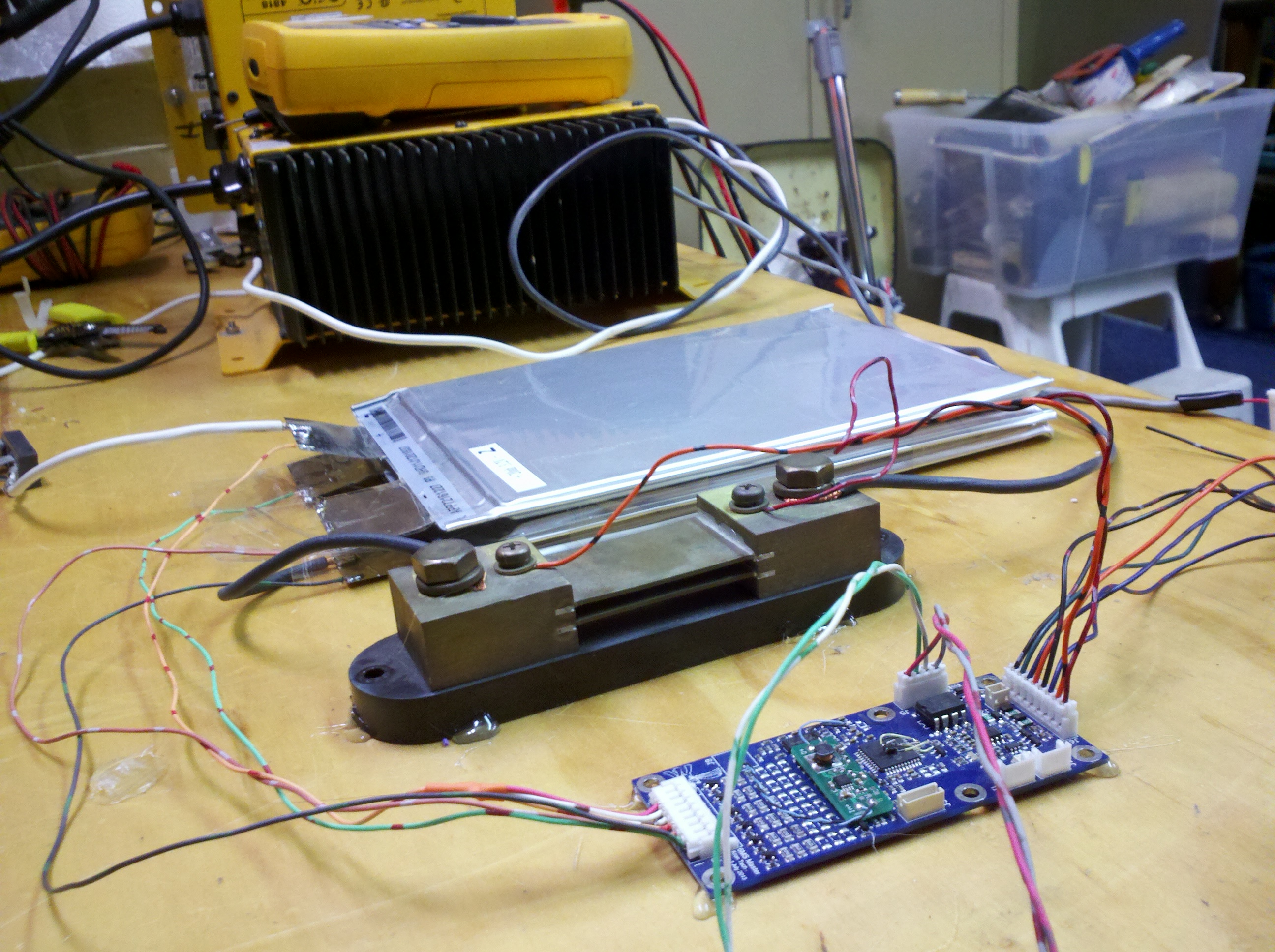
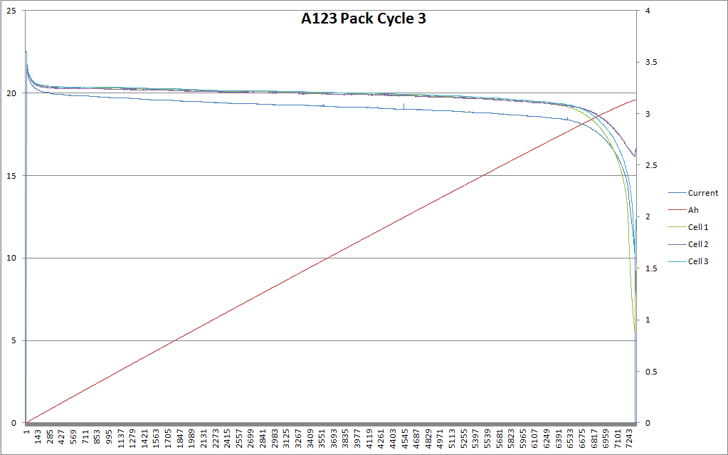
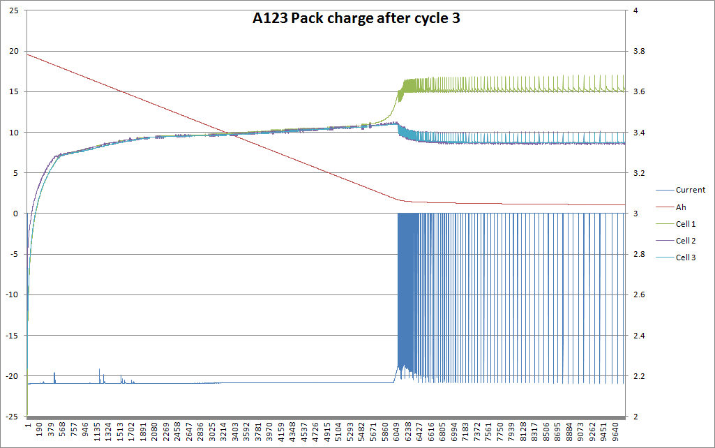
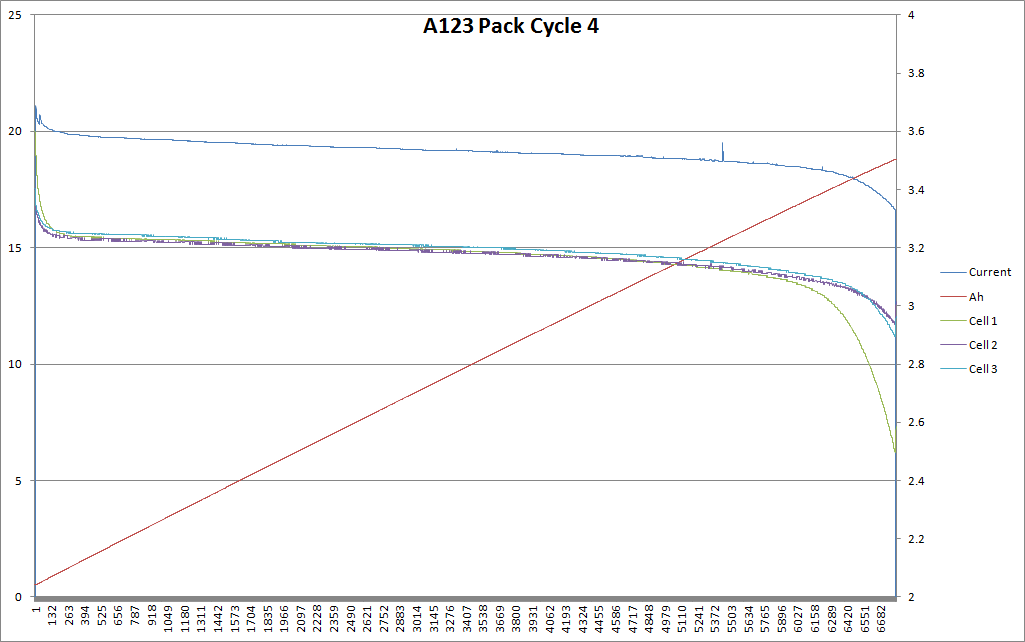
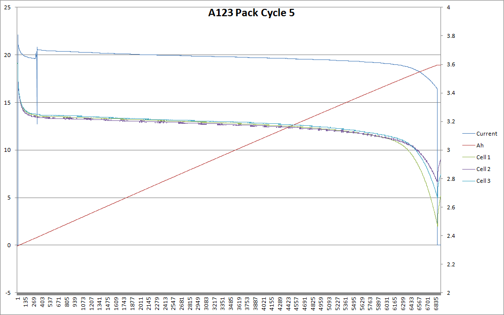
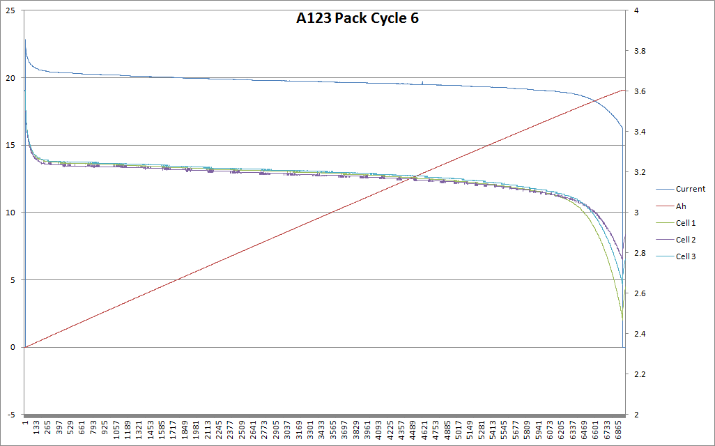
The 3 cells are now assembled into a pack, which will speed up testing compared to doing each individually.
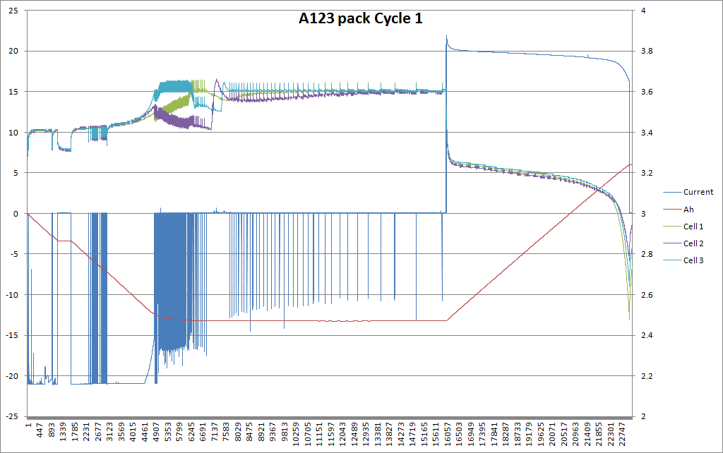
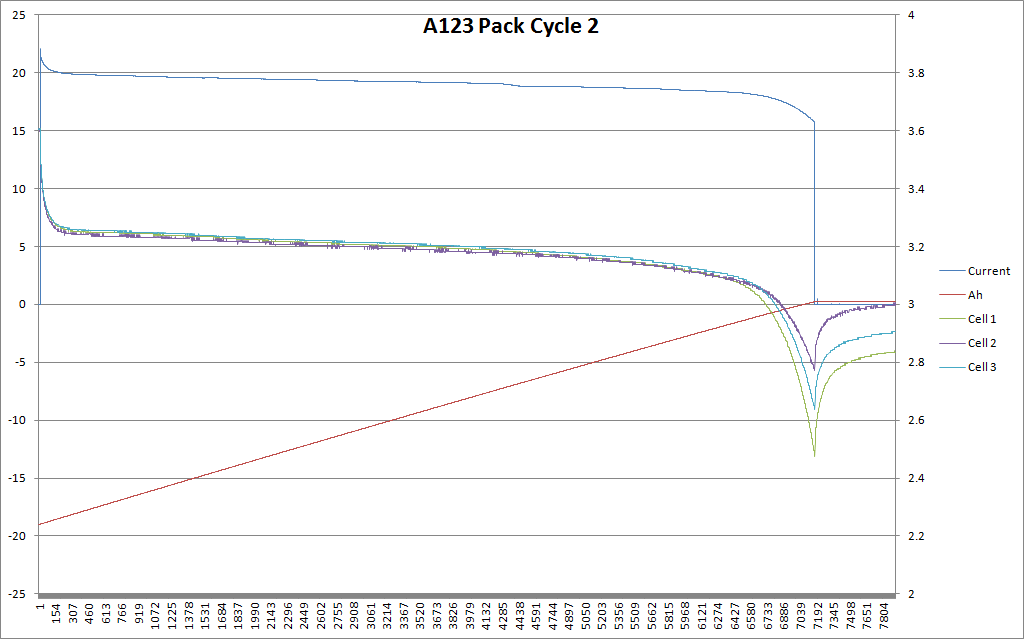
6 cycles have been performed on the pack so far, and the performance has been consistently around 19Ah. On cycle 3 the pack was accidentally over discharged, causing a temporary reduction in capacity that appears to be recovering over several cycles.
Notes
1. Accidentally overdischarged to <1Vpc on cell 1. Ah value includes discharge only to 2.5Vpc
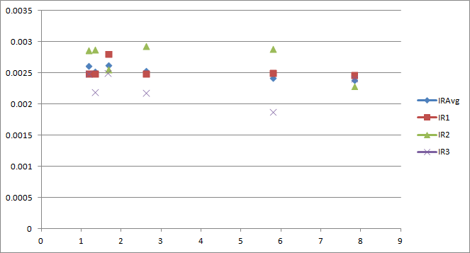
The cell internal resistance averages 2.5mOhm with some spread over time and cell that’s measured. The load was varied from 20A to 36A and voltage deltas used to calculate the internal resistance. X axis on the graph below is Ah discharged from full charge.
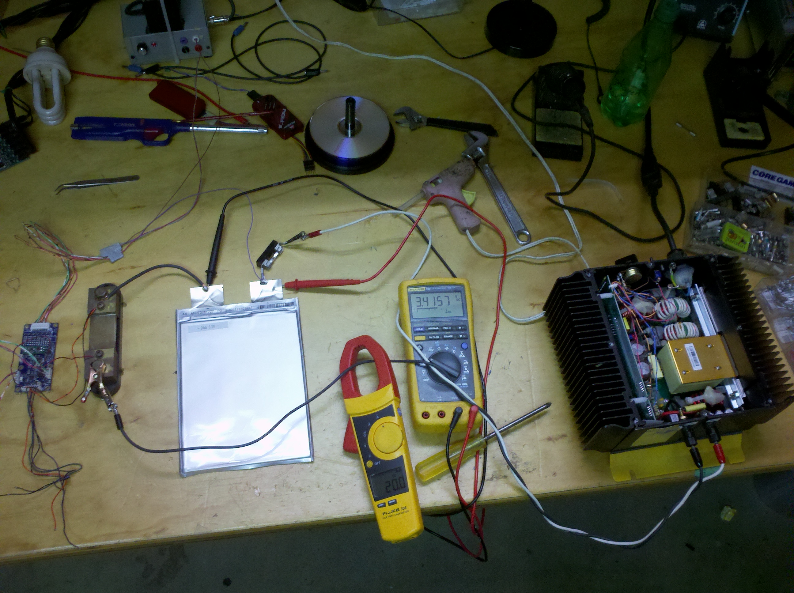
I’m designing a battery for our go-kart team ArcWolf Racing. Basic specs are around 88V and 30-40Ah, and one of the prime candidates are the 3.2V 20Ah A123 pouch cells, configured at 28S2P for 89.6V 40Ah. Local sources are about $70 per cell which is very high compared to the ~$20-30 per cell available on Alibaba or AliExpress.
After looking at reviews, the seller ShenZen FHT Co. Ltd. has the best feedback, so we ordered 3 cells for testing at $30 each. They arrived within 2 weeks and were packed well (box in a box in a box!).
The test setup consists of a modified Delta-Q charger acting as a power supply, a shunt, one of my BMS prototypes as a data logger for voltage and current, and a “MacGyver” resistor consisting of bailing wire in a bucket of water.
Figure 1 – Test setup
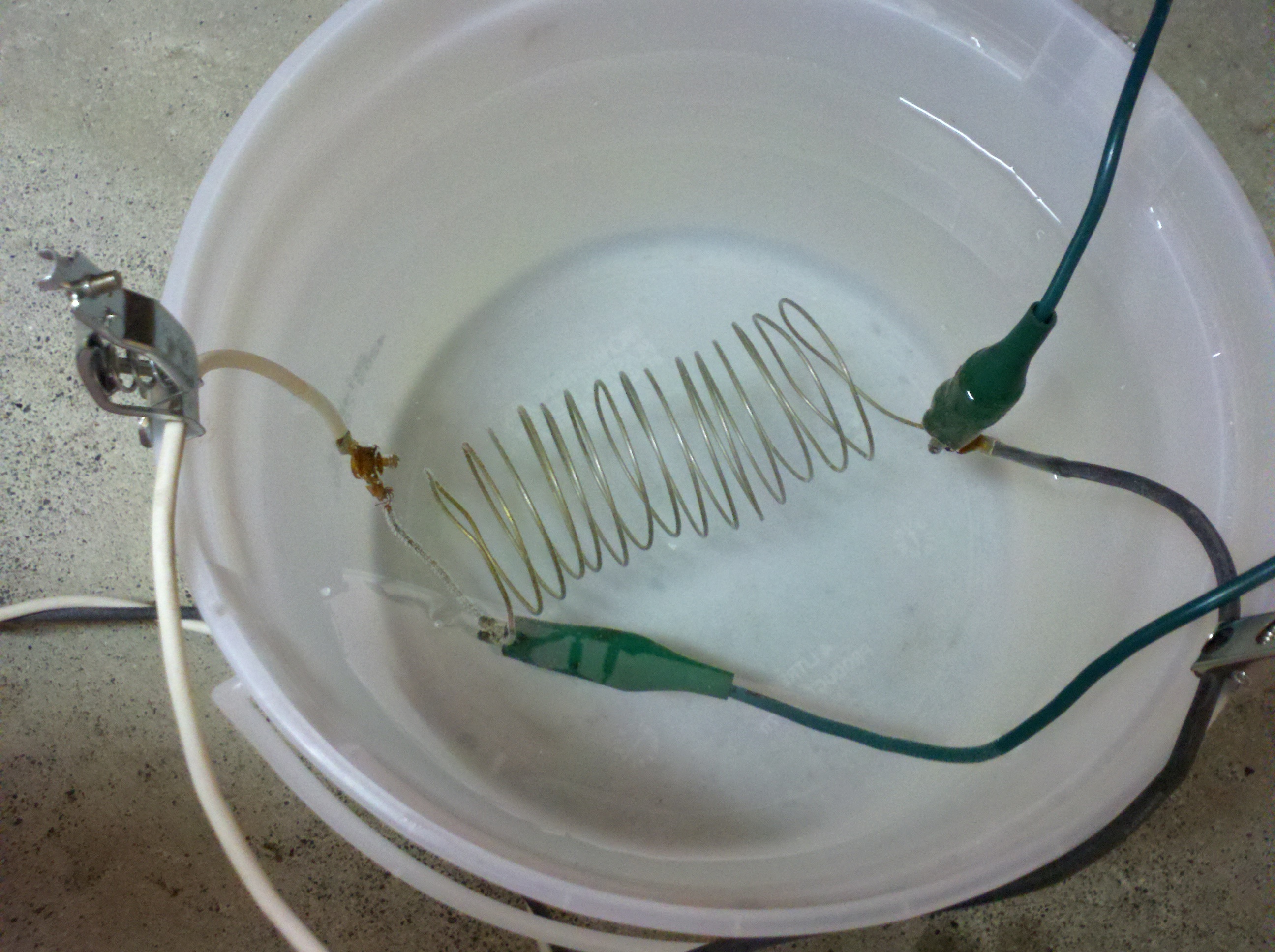
Figure 2 – “MacGyver” resistor with resistance controlled by moving green alligator clip tap
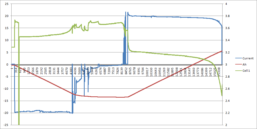
Cell 1 was charged to full capacity at 1C (20A) to 3.6V, putting 13.5Ah into the cell from its shipping state of charge. It was then discharged using the resistor down to 2.5V, resulting in 19Ah capacity.
Figure 3 – Cycle 1 on Cell 1, starting from shipping SOC. Total discharge 19Ah. Raw data: Cell 1 cycle 1
A quick test of the internal resistance was performed, which is probably highly inaccurate. The voltage drop from rest was measured when a 25A load was connected, resulting in a 50mV drop, putting the internal resistance at about 2mOhm.
Further testing to follow with more cycles on more cells. Looking promising initially though!


![MriMt[1]](http://omeganaught.com/wp-content/uploads/2014/10/MriMt1.jpg)
![lpogu[1]](http://omeganaught.com/wp-content/uploads/2014/10/lpogu1.jpg)