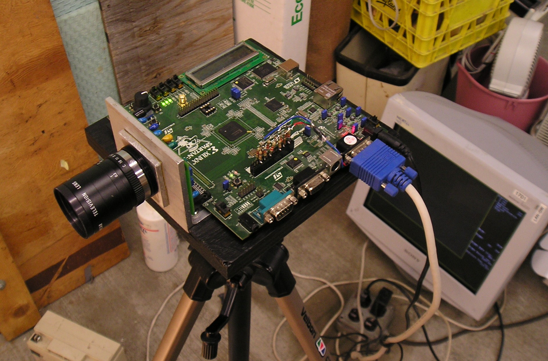
The HSC80 was a fun project, but suffered from speed limitations, as well as a limitation facing almost all high-speed cameras: it requires a PC to fully operate and save videos. From the beginning of the HSC80 project I was intending to use the LUPA1300-2 image sensor in a camera. This sensor is about 10x faster than the HSC80’s LUPA 300, capable of 1280×1024 at 500fps as well as higher speeds at lower resolutions, beyond 2000fps at 640×480 for example.
The name HS768, like the HS80, refers to the data rate of the image sensor, which is 768Mpix/s, or about 960MB/s once the 10 bit data format is considered.
Since I didn’t have my website up when I started this project, these first few posts will be a quick overview of the progress of the project.
Design Goals
Going into this project, I wanted to create a high-speed camera that operated like any consumer camera would, as well as doing what normal high-speed cameras do. It had to:
- Fit into a comfortable handheld format
- Operate standalone with built-in UI – fully operable without tethering to a PC
- Save video to removable media (SD card, USB, SATA drives)
- Save to compressed formats directly using modern compression (h264) as well as uncompressed formats
- Be controllable remotely via Ethernet, as these cameras are sometimes used near things you don’t want to be near (exploding things, flying debris, etc)
- Build for less than $3k parts per camera
Design
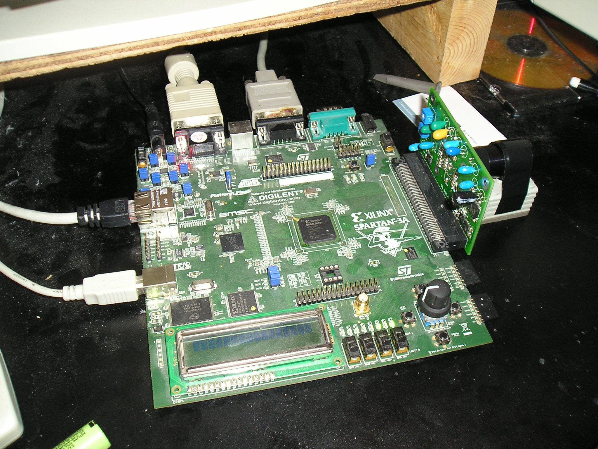
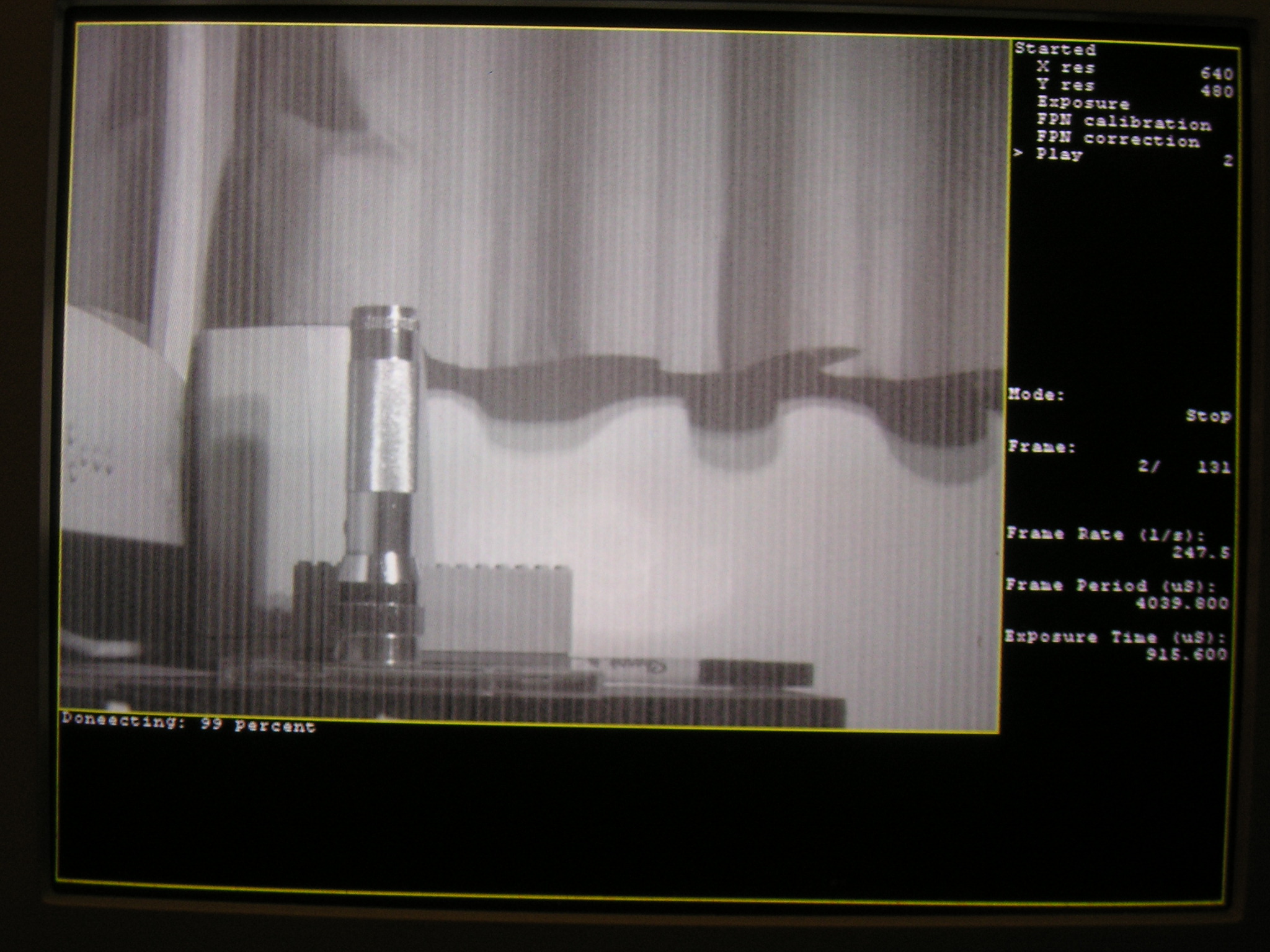
Originally the entire system was going to be built into an FPGA, and this is how I built the initial prototype:
I quickly realized the software would be a massive project. Supporting various filesystems for removable media (FAT, NTFS (because who likes 4GB file size limits?), EXT3) would be a massive and time consuming software challenge. Implementing h264 compression in an FPGA is also a formidable challenge unless you buy an off-the-shelf IP core, and the performance is limited in low-end FPGAs.
The solution to these problems is simple. Let someone else do all the hard work!
How do you do that (without paying someone)? Take advantage of open source, running Linux on top of a SOC (system-on-chip) video processing IC, something that would typically be used in digital video recorders, security systems, cameras, etc. Linux takes care of the pesky details of storage support, and the SOC and associated drivers provide hardware h264 encoding as well as support for all the Linux niceties without having to write drivers.
As a side benefit, adding a SOC actually reduces the system cost, because FPGA space very expensive compared to an ASIC, so the smaller FPGA more than makes up for the added cost of the SOC.
Enter Davinci
SOCs are notoriously “protected” by their manufacturers, case in point the Raspberry Pi. The Pi’s SOC datasheets are only available from the manufacturer under NDA, and they usually won’t even talk to you unless you’re purchasing huge quantities of parts. The parts usually have short lifespans, for example SOCs used in phones may remain in production for a year or less. There are a few exceptions to this rule, mainly some parts released by TI and Freescale. The industrial segment of the market usually has longer production lifetimes, with TI claiming that they will not obsolete a part if anyone orders it within 3 years. That claim should probably be taken with a grain of salt however.
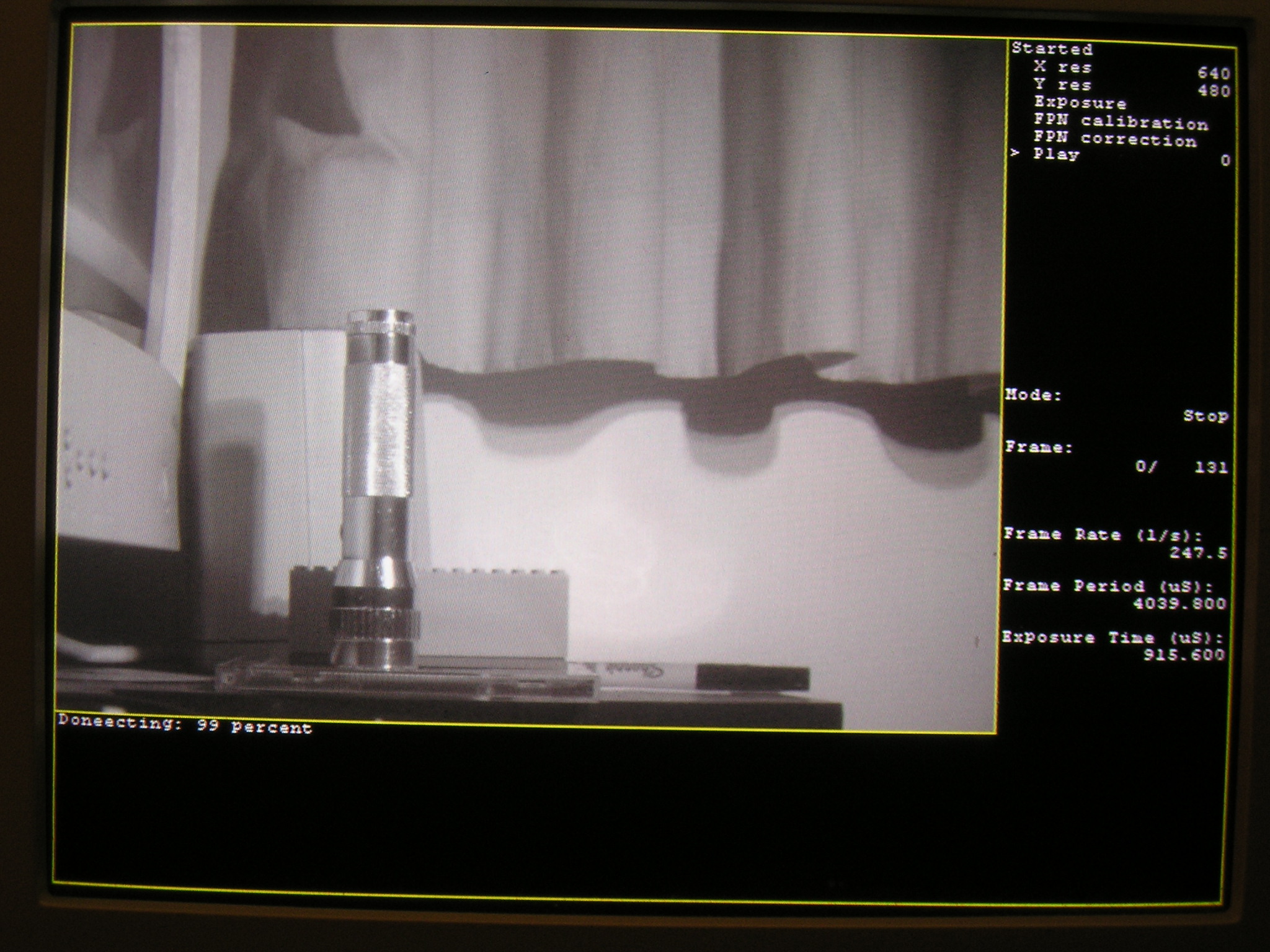
The speed at which you can save video is limited by the speed of the memory card or video compression, so the faster the better. At the time of selection, the fastest single channel h264 compression in an industrial part was the DM814x series from TI’s Davinci line. The DM8148 supports 1080p60 compression in real time, and has other nice features like a 1GHz CPU (ARM, not that architecture really matters), USB host, SATA, HDMI, multiple video ports, etc. Just the ticket! Software support is provided with a TI Linux branch with all their drivers built in.
DDR3 woes
High speed cameras usually store data to a RAM buffer due to the high data rate, although some manufacturers offer ludicrously expensive custom SSDs that allow shooting at partial rates for long durations. DDR3 RAM is the logical choice as it’s abundant and cheap, especially in DIMM/SODIMM format. Unfortunately most FPGAs only support components (RAM chips mounted directly on the board), not full modules. Due to the consumer market for modules, ordering a single chip can cost almost as much as an entire module which could contain 8 or 16 chips, so there’s serious pressure to use modules.
Neither Altera nor Xilinx support DDR3 modules in an FPGA costing less than $1k. One manufacturer, Lattice, does offer DDR3 DIMM/SODIMM support in their ECP3 series, and this was the driving force in selecting the ECP3 for the camera.
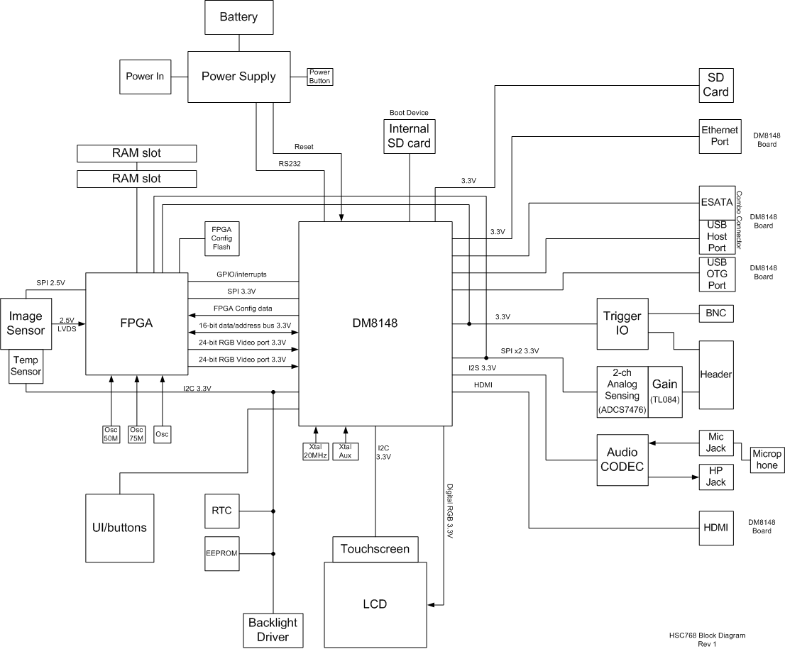
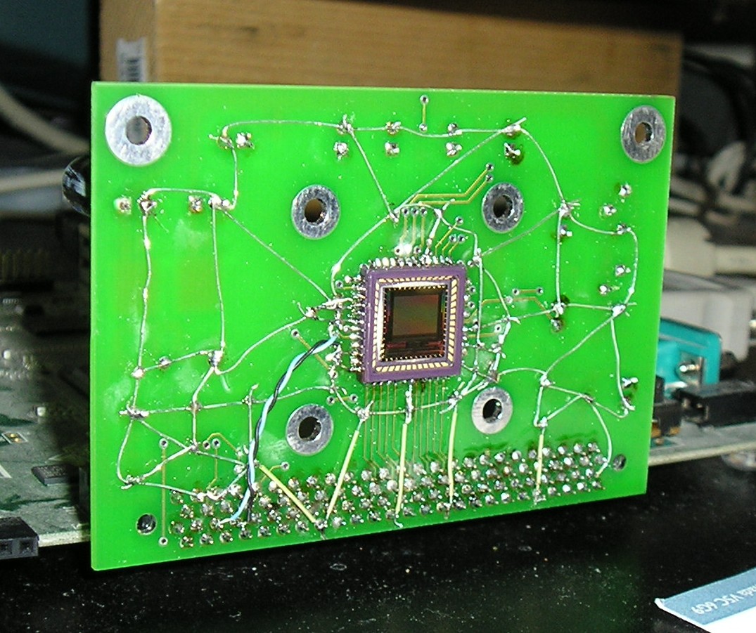
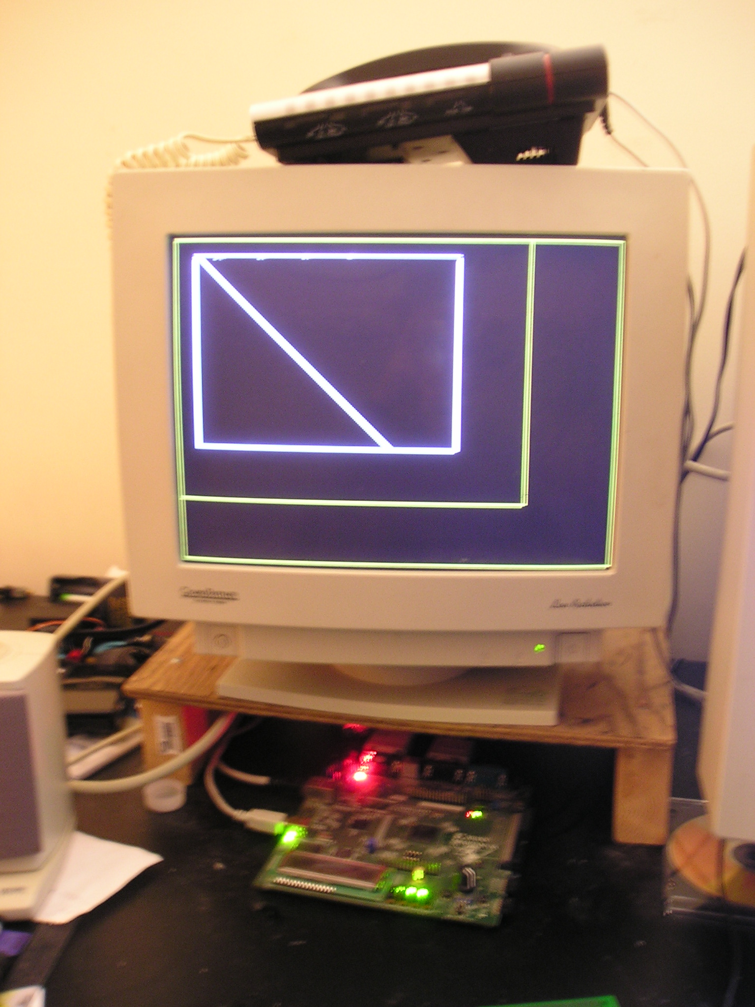
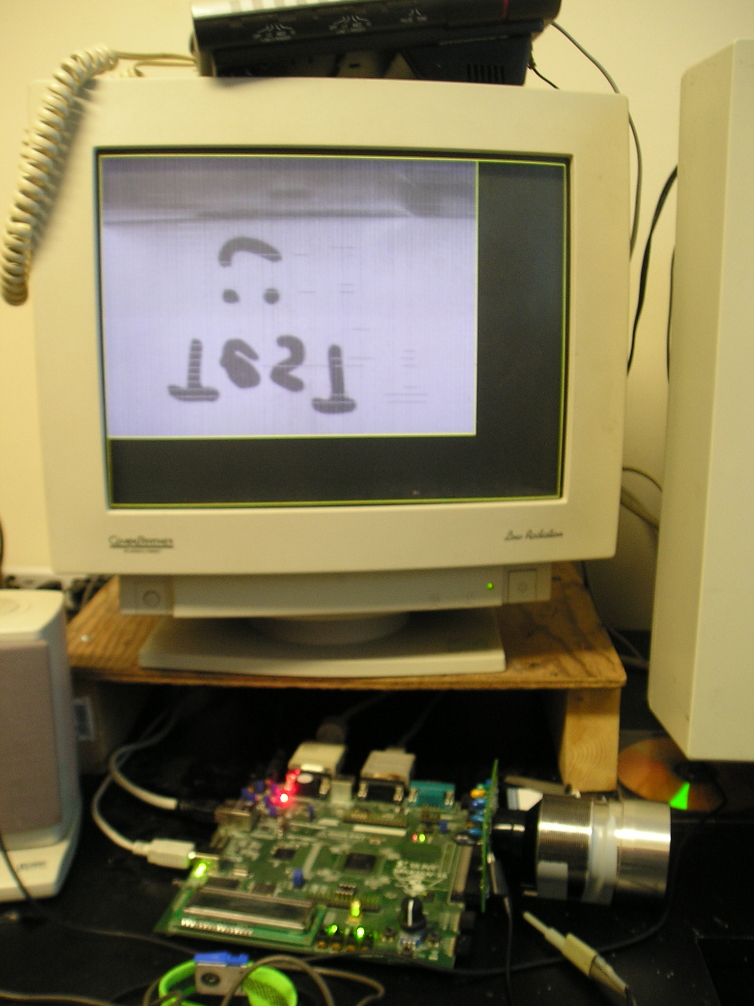
Archetecture
The camera is basically split into two sections. An FPGA handles data acquisition from the image sensor, storing the data into 16GB of DDR3 RAM, allowing about 20s of record time at full speed. The FPGA converts the raw sensor video into a fully processed RGB video stream which is sent to the DM8148.
The DM8148 takes care of saving the video stream, and controls the whole system, proving all the niceties you get on a modern PC: Graphics, HDMI, USB, SATA, SD cards, etc.
Board Layout
I didn’t document the layout process in great detail, but I did get a nice timelapse of the DDR3 memory layout for the DM8148:
DDR3 Routing Part 1
DDR3 Routing Part 2
And here are the current prototype boards finished:
![MriMt[1]](http://omeganaught.com/wp-content/uploads/2014/10/MriMt1.jpg)
![lpogu[1]](http://omeganaught.com/wp-content/uploads/2014/10/lpogu1.jpg)
Stay tuned for more project history!